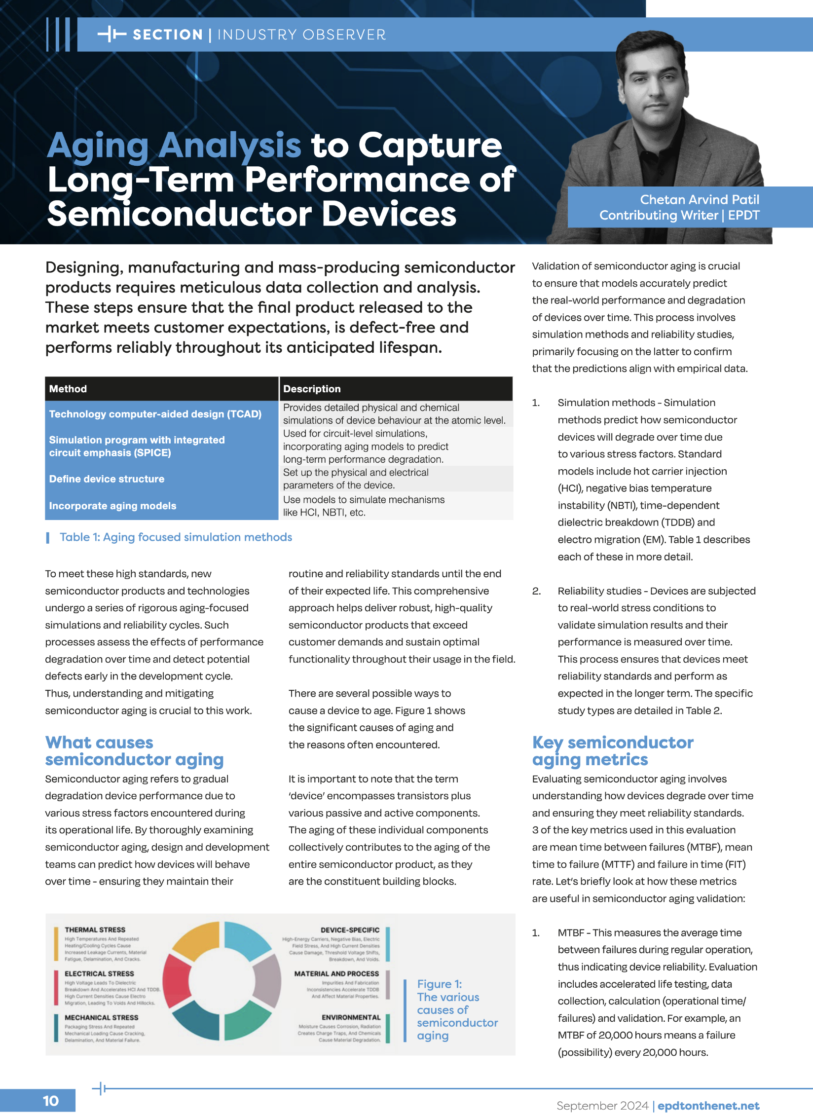
Image Generated Using DALL-E
The Surge In Fab Construction
It is no secret that the semiconductor industry is seeing an unprecedented boom in FAB construction. We are not talking about incremental growth. We are witnessing a monumental shift in how and where these crucial facilities are built.
Over 80 new FAB projects are underway or planned to be operational by 2024. This is not just a blip on the radar but a transformative wave sweeping across the globe. From Arizona to Taiwan, governments and corporations are investing billions to build new semiconductor manufacturing facilities to fortify supply chains and secure a more resilient future for tech.
This surge is more than just numbers. It is a strategic realignment of the global semiconductor landscape. The new FABs are producing more chips and enabling the next generation of technologies. Think about the chips powering electric vehicles, AI, and high-performance computing. The industry is gearing up to meet the demands of a future heavily reliant on advanced semiconductors, and this construction frenzy is setting the stage.
But the question remains – can this pace of construction and expansion be sustained? Is the industry building too many FABs too quickly, risking overcapacity and financial instability? Or is this surge necessary to future-proof our technology-dependent world against supply chain disruptions?
Now, let us explore a few key aspects to understand the dynamics at play better.
Driving Forces Behind The Surge
Several key factors are driving this massive expansion. First and foremost, we have the post-pandemic reality check. The global chip shortage during the pandemic revealed how vulnerable the semiconductor supply chain is. Suddenly, everyone – from governments to automakers – realized the critical importance of having a reliable, domestic chip supply. This was a wake-up call, and the world is now scrambling to ensure that a chip shortage does not cripple entire industries again.
Then, there is the relentless demand for more advanced technology. The rise of AI pushes the envelope on what semiconductor manufacturers can deliver. On top of that, today’s chips need to be smaller, faster, and more efficient than ever. Thus demanding new fabs and nodes.
This kind of innovation requires cutting-edge FABs capable of producing chips at nodes smaller than 7nm. Thus, governments are putting their money where it is worth, with the U.S. CHIPS Act and similar initiatives in Europe and Asia injecting billions into semiconductor manufacturing.
Lastly, geopolitical factors cannot be ignored. The trade war and the desire to reduce dependency on a few critical regions for chip production are pushing countries to localize their semiconductor manufacturing. This is not just about economics but also national security and technological sovereignty.

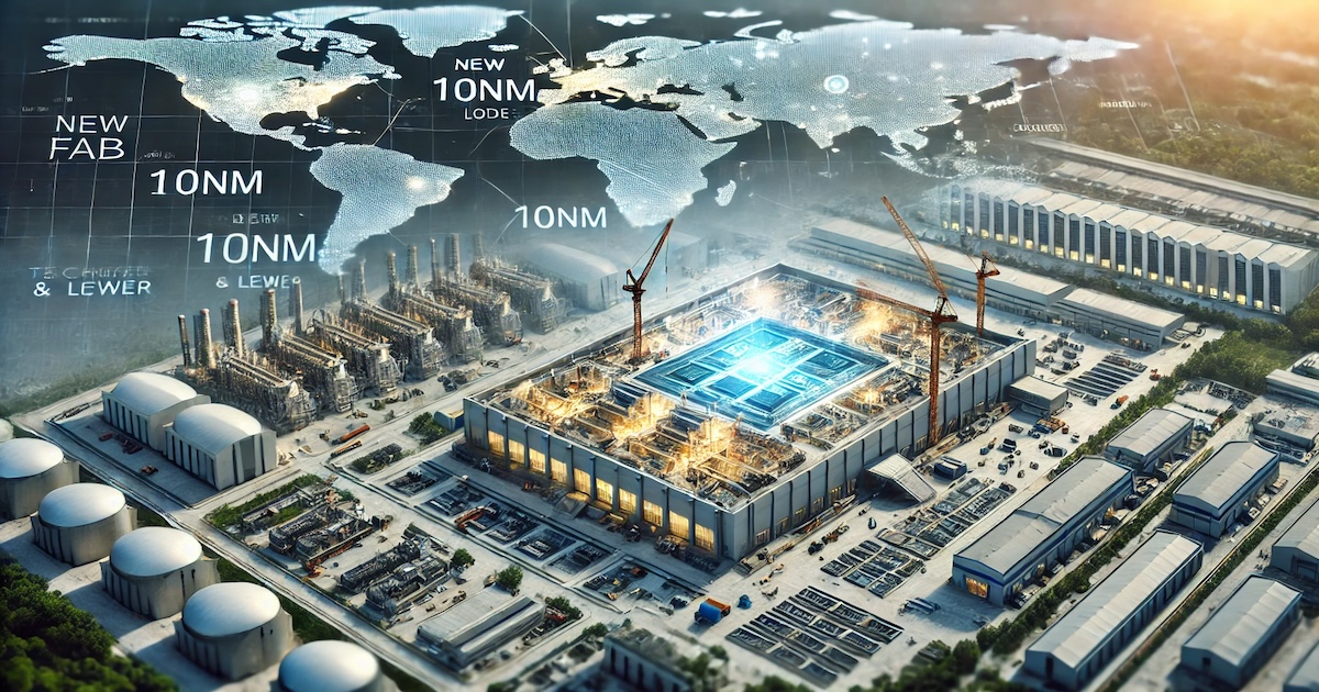
New Fab Geography
The geography of semiconductor manufacturing is changing dramatically. Traditionally, most of the world’s semiconductor manufacturing has been concentrated in East Asia, with Taiwan, South Korea, and China leading the charge. While these regions are still at the forefront, new players are emerging.
The U.S., for example, is making a serious comeback. Thanks to the CHIPS Act, states like Arizona, Texas, and Ohio are becoming hotbeds for new FAB construction. Intel, TSMC, and Samsung invest heavily in U.S. soil, building state-of-the-art facilities at 5nm and below advanced nodes.
Europe, too, is stepping up its game. The European Union has its version of the CHIPS Act, aiming to double its share of global chip production by 2030. Countries like Germany and Ireland are seeing new investments from giants like Intel and GlobalFoundries. These new FABs are not just expanding capacity but are strategically positioned to reduce dependency on Asia.
Emerging markets like India are also making significant strides in the semiconductor industry. While India is yet to become a major player in FAB manufacturing (maybe beginning in 2025, it will), it is also investing in backend processes like assembly and testing. The country strategically positions itself as a crucial part of the semiconductor supply chain, leveraging its robust engineering talent pool. This development is a promising sign for the future of the global semiconductor industry.
Challenges And Potential Pitfalls
While the surge in FAB construction is promising, it has challenges. First, there is the issue of overcapacity. The semiconductor industry is notoriously cyclical. When demand is high, everyone rushes to build capacity, but when demand dips, we could see many of these new FABs running below capacity, leading to financial strain.
Remember the solar panel boom of the 2000s? Overcapacity led to a massive market crash. The semiconductor industry needs to avoid a similar fate.
The talent shortage is another critical issue. Building and operating a semiconductor FAB requires highly specialized skills, and there are not enough qualified engineers and technicians to go around. The U.S. alone is projected to have a shortfall of 300,000 engineers over the next decade. This shortage could delay the completion of new FABs and affect their operational efficiency once they’re up and running. However, by investing in education and training, we can address this shortage and ensure a skilled workforce for the future.
Then there is the supply chain. Building an FAB is just one piece of the puzzle. It would help if you also had a robust supply chain for raw materials, equipment, and backend services like assembly and testing. Currently, most of these services are concentrated in a few regions, which could create bottlenecks and undermine the resilience that new FABs are supposed to provide.

Economic And Strategic Implications
The economic and strategic implications of this FAB surge are enormous. On the financial front, these new facilities are not just creating tens of thousands of high-paying jobs and attracting billions in investment but also creating a ripple effect across various sectors, from construction to high-tech services. This is a boon for local economies, fostering optimism and a sense of growth, and will profoundly impact the overall economic landscape.
Strategically, increasing semiconductor manufacturing capacity is about much more than just chips. It is about national security and technological leadership. Countries are keen to reduce their dependency on a few key players for critical technologies.
For the U.S., this surge is a chance to reclaim its position as a leader in semiconductor manufacturing. For Europe, it is a way to secure its technological sovereignty. And for China, it is about self-sufficiency in the face of export controls and trade restrictions. For India, it is about emerging as a new leader in the semiconductor ecosystem.
In conclusion, while the surge in semiconductor FAB construction is an exciting development, it has risks. The industry must manage this expansion with caution, carefully avoiding overcapacity and ensuring it has the talent and supply chain infrastructure to support these new facilities. If done right, this could mark a new era of resilience and innovation for the semiconductor industry. If not, we could be setting ourselves up for another boom-bust cycle.