Published By: Electronics Product Design And Test
Date: June 2024
Media Type: Online Media Website And Digital Magazine
Blog
-

Hidden Dangers: Understanding And Preventing The Counterfeiting Of Semiconductor Products
-

The Semiconductor Talent Demand In India
Image Generated Using DALL-E
India And Semiconductor
India’s semiconductor industry is on the cusp of a significant transformation, driven by a huge demand for talent and rapid technological advancements. With 2.55 million STEM graduates yearly, India ranks second globally in producing Science, Technology, Engineering, and Mathematics graduates.
As the world increasingly relies on semiconductors for everything from smartphones to electric vehicles, India’s role as a key player in this global ecosystem becomes increasingly critical.
Thus, exploring the multifaceted dynamics of the demand for semiconductor talent in India is essential, shedding light on the historical context, current landscape, and the factors fueling this demand.
Semiconductor Background In India
India’s journey in the semiconductor industry began in the late 20th century, marked by the establishment of key research institutions and the advent of multinational semiconductor companies setting up operations in the country. Initially, India’s role was primarily confined to software services and design, leveraging its strong IT industry.
Over the years, however, the landscape has evolved. Government initiatives, such as the Make in India campaign and semiconductor fabrication labs’ establishment have been pivotal in fostering a more comprehensive semiconductor ecosystem. Today, India is a hub for semiconductor design and makes strides in manufacturing and research, positioning itself as a critical player in the global supply chain.
STEM Graduates In India
India is a powerhouse in STEM education, with more than 2.55 million graduates yearly, second only to China. This significant pool of STEM talent positions India as a crucial player in the global semiconductor industry. The abundance of skilled graduates from Indian universities ensures a steady supply of engineers, researchers, and technicians to fuel the semiconductor sector’s growth.
India’s prominence in STEM education underpins its potential to address the global semiconductor talent shortage. As the industry evolves with advancements in AI, the demand for highly specialized knowledge and skills increases. Indian STEM graduates, equipped with strong technical backgrounds, are thus well-suited to meet these needs, driving innovation and efficiency in semiconductor design and manufacturing.

Image Credit: CSET
Moreover, India’s educational institutions and government initiatives foster an environment conducive to technological advancements. Partnerships between academia and industry, alongside government incentives, are crucial in enhancing the skill sets of Indian STEM graduates, making them even more valuable to the semiconductor industry.
In the near-term, India’s substantial number of STEM graduates will play a pivotal role in the semiconductor sector. Leveraging this talent pool can significantly impact global semiconductor supply chains, ensuring sustained innovation and competitiveness in this critical field.
Factors Driving Semiconductor Growth In India
Understanding the factors driving the demand for semiconductor talent in India is crucial to appreciating the industry’s growth dynamics. Government initiatives, which are significant, market growth, which is promising, technological advancements, and the push for self-reliance are all playing pivotal roles in shaping this demand.
These elements collectively create a fertile ground for the semiconductor sector to flourish, necessitating a diverse and skilled workforce.
Factor Description Government Initiatives Policies such as the Production Linked Incentive (PLI) scheme and Electronics Manufacturing Clusters (EMC) scheme aim to attract investments and boost local production capabilities, fostering a conducive environment for semiconductor companies. Market Growth The global semiconductor market is expanding due to the proliferation of digital technologies like AI. This growth increases the demand for skilled professionals to design and manufacture semiconductors. Technological Advancements Emerging technologies require advanced semiconductor solutions, driving the need for highly skilled workers. Indian educational institutions are focusing on these technologies, producing graduates equipped to meet industry needs. Self-Reliance Efforts to reduce dependency on foreign semiconductor imports and enhance local capabilities drive demand for skilled talent. Initiatives to promote domestic semiconductor manufacturing and design are crucial in achieving self-reliance.

Picture By Chetan Arvind Patil
Areas Of Semiconductor Talent Demand
Understanding the areas where talent demand is most pronounced in the semiconductor industry is paramount. By delving into the various domains – design, manufacturing, and RnD – one can pinpoint the skills and expertise in high demand.
This detailed examination will highlight the critical roles and opportunities available, shedding light on how India’s educational institutions and industry partnerships prepare to meet these demands.
Section Details Areas Of Talent Demand Design: Demand for roles such as design engineers, verification engineers, and system architects has surged, driven by AI and computing advancements.
Manufacturing: Rising demand for process engineers, equipment engineers, and technicians due to government initiatives and new fab setups.
RnD: High demand for materials science, quantum computing, and nanotechnology researchers to drive innovation.Education And Skill Development Educational Institutions: Premier institutions like IITs, NITs, and leading universities offer specialized electronics and engineering programs.
Skill Gaps: Additional training in VLSI design, semiconductor fabrication, and advanced materials science is needed.
Industry-Academia Collaboration: These partnerships, fostering sponsored research, internships, and workshops, are key to aligning academic programs with the dynamic needs of the industry, leading to a more skilled workforce.Challenges Brain Drain: The migration of skilled professionals abroad for better opportunities; the need to create attractive work environments in India.
Infrastructure: There is a need for substantial investment in advanced machinery and facilities for semiconductor fabs and research labs.
Retention: Competitive salaries, a positive work culture, continuous learning, and clear career progression are essential to retain talent.Opportunities And Future Outlook Startups and Innovation: Emergence of startups focusing on AI, IoT, and specialized semiconductor applications, supported by government initiatives.
Global Competitiveness: The industry’s strength lies in its ability to leverage highly skilled professionals, a robust education infrastructure, and unwavering government support, all of which are propelling it towards becoming a semiconductor global leader.
Long-term Strategies: The industry is committed to a path of continuous investment in education, infrastructure, and industry collaboration, bolstered by policies that foster innovation and ease of doing business.Take Away
For sure, India is pivotal in the global semiconductor industry, driven by a robust educational infrastructure, supportive government policies, and a market demand. The nation’s significant pool of STEM graduates positions it to meet the growing global and domestic demand for semiconductor talent. However, challenges such as brain drain, infrastructure limitations, and retention issues must be addressed to fully capitalize on this potential.
By fostering solid collaborations between industry and academia, investing in advanced training programs, and creating a conducive work environment, India can bridge the existing skill gaps and enhance its competitiveness on the global stage. The rise of startups and innovation hubs, supported by government initiatives, further underscores the country’s potential to lead in semiconductor design, manufacturing, and RnD.
Long-term strategies focusing on continuous investment in education, infrastructure, and policy support are essential to sustain and grow the semiconductor talent pool. As India navigates these challenges and opportunities, it is well-positioned to become a global powerhouse in the semiconductor industry, driving innovation and economic growth for years.
-

Optimizing Semiconductor Product Development: Chetan Arvind Patil On Yield, Testing, And Industry Impact
Published By: Silicon India
Date: 14th June 2024
Media Type: Digital -

The Act Of Balancing Semiconductor FAB Race By Focusing On Process Flavor Over Process Node
Image Generated Using DALL-E
Semiconductor Node Race
The semiconductor industry has long been dedicated to achieving exceptional performance, efficiency, and cost-effectiveness, primarily by advancing smaller process nodes. However, the increasing physical and economic challenges of further node shrinking have prompted a strategic shift in focus.
This exciting shift, known as ‘process flavor, ‘is not just a change in direction but a potential game-changer for the semiconductor industry. It involves the development of customized process technologies that are finely tuned for specific applications, marking a significant departure from the previous node-centric approach. With its potential to completely transform the industry, this innovative approach holds great promise for the future.
Process Flavor Vs Process Nodes
In the traditional semiconductor landscape, the drive towards smaller process nodes has been the hallmark of progress, symbolizing advancements in miniaturization, speed, and power efficiency. The smaller the node, the more transistors can be packed onto a chip, leading to higher performance and lower power consumption. This relentless pursuit, governed by Moore’s Law, has propelled the industry through remarkable technological milestones, with current leading-edge nodes reaching 3nm and 2nm. However, pursuing smaller nodes is becoming increasingly fraught with challenges, including astronomical RnD costs, manufacturing complexities, and diminishing returns in performance and efficiency gains.
Conversely, process flavor ushers in a new era in semiconductor manufacturing. Instead of fixating on the most minor possible node, process flavor advocates for customizing process technologies to meet specific application needs. This approach acknowledges that different applications, from high-performance computing to low-power devices, have unique requirements that can only be met through specialized process optimizations rather than a universal node shrinkage. By tailoring processes to specific use cases, manufacturers can achieve significant improvements in performance, cost efficiency, and energy consumption, all while mitigating the mounting challenges associated with node scaling. This strategy enhances technological versatility and market responsiveness and fosters innovation in areas where traditional node-focused approaches may need to be more effective.

Picture By Chetan Arvind Patil
Key Features Of Process Flavor And Nodes
As the semiconductor industry evolves, manufacturers’ strategies are diversifying to meet a variety of technological and market demands. Traditionally, the focus has been on shrinking process nodes to achieve higher performance and efficiency.
However, the emerging strategy of process flavor, which involves tailoring semiconductor manufacturing processes to specific application requirements, is gaining traction. This comparison table highlights the key differences between process flavor and process nodes, illustrating how each approach impacts various aspects of semiconductor technology and manufacturing.
Feature Process Flavor Process Node Definition Customizing semiconductor processes for specific applications Shrinking transistor size to achieve smaller nodes (e.g., 7nm, 5nm, 3nm) Focus Application-specific optimizations Achieving the smallest possible transistor size Cost Efficiency Generally more cost-effective for targeted applications Higher RnD and manufacturing costs due to complexity Performance Tailored performance for specific use cases (e.g., power efficiency, speed) Higher performance potential through increased transistor density Complexity Increased design and manufacturing complexity due to customization High complexity due to advanced lithography and fabrication techniques Market Adaptability Flexible and responsive to diverse market needs Primarily driven by leading-edge markets and high-volume applications Sustainability Can optimize for energy efficiency and resource usage High energy consumption and environmental impact at advanced nodes RnD Investment Focused on developing multiple specialized processes Large investments required for each new node generation Technological Challenges Balancing customization with manufacturing feasibility Physical and economic limits of silicon technology Innovation Encourages innovation in diverse application areas Innovation primarily in lithography and transistor scaling Adopting a process flavor approach allows semiconductor manufacturers to tailor their technologies to meet the diverse demands of various applications, ranging from high-performance computing to energy-efficient devices. This strategy can lead to more sustainable practices and potentially lower development costs, as it avoids the escalating complexities associated with further node shrinking.
While process nodes have propelled significant technological progress, the transition to process flavor signifies a nuanced comprehension of market demands and technological capabilities. By harmonizing these two approaches, manufacturers can sustain innovation and deliver optimized solutions that precisely match the requirements of diverse applications, thereby fortifying the semiconductor industry’s resilience and adaptability.
Take Away
As the semiconductor industry navigates the challenges of advancing node shrinking, focusing on process flavor offers a balanced and strategic approach. By optimizing manufacturing processes for specific applications, semiconductor manufacturers can achieve significant performance and efficiency gains while managing costs and complexity. This shift addresses the limitations of pursuing ever-smaller nodes and paves the way for more sustainable and diversified technological advancements in the semiconductor industry.
-
Beyond Moore: Design and Manufacturing Challenges In System-On-A-Wafer
Published By: Commercial Micro Manufacturing
Date: June 2024
Media Type: Digital Media -

The Semiconductor Manufacturing Training Through Virtualization
Image Generated Using DALL-E
Semiconductor And Virtualization
In the ever-evolving landscape of semiconductor manufacturing, staying ahead of technological advancements and maintaining a highly skilled workforce is critical for success. While effective, traditional training methods often have significant costs, safety concerns, and accessibility limitations. Enter virtualization – a transformative approach that has revolutionized how the industry and academia train and educate individuals in the semiconductor industry.
Virtualization leverages advanced technologies to create immersive, interactive, and highly realistic simulations of semiconductor manufacturing processes. Doing so offers many benefits that traditional methods cannot match.
Application Of Virtualization In Semiconductor
By leveraging advanced technology to create immersive and interactive environments, virtualization offers unparalleled learning and skill development opportunities. This innovative approach addresses many challenges associated with traditional training methods, providing a safer, more cost-effective, and flexible alternative.
As the semiconductor industry advances rapidly, the need for up-to-date and comprehensive training programs becomes increasingly critical. Virtualization, with its inherent adaptability, meets this demand by enabling efficient, scalable, and highly effective training solutions.
Below are some key applications of virtualization in semiconductor training, highlighting how it enhances the learning experience and prepares trainees for real-world scenarios:
Application Details Process Simulation Trainees can experience and optimize various manufacturing processes in a risk-free virtual environment. Equipment Operation Training Virtual models of complex machinery help trainees learn how to operate and troubleshoot equipment effectively. Cleanroom Protocols Simulating cleanroom conditions allows trainees to practice maintaining contamination-free environments. Data Analysis And Visualization Virtual tools teach trainees how to interpret and act on process data. Quality Control Virtual environments replicate quality control scenarios, enabling trainees to identify defects and implement quality assurance measures. Design And Fabrication Techniques Virtual platforms provide detailed simulations of design and fabrication techniques, enabling learners to understand and implement advanced methods. Supply Chain Management Virtual training includes modules on managing supply chains, understanding logistics, and optimizing the flow of materials in semiconductor manufacturing. Educational Courses And Certifications Virtual platforms offer comprehensive courses and certification programs, ensuring learners are up-to-date with the latest industry standards. Collaborative Projects Students and professionals can work together on virtual projects, simulating real-world collaboration and problem-solving scenarios. Virtual Reality Classrooms Immersive virtual reality classrooms enhance the learning experience by providing interactive and engaging educational content. Remote Laboratory Access Virtualization allows for remote access to laboratory experiments and equipment, enabling students to conduct experiments and gather data remotely. Interactive Tutorials And Workshops Virtual environments host interactive tutorials and workshops, allowing learners to gain practical skills through hands-on activities. Performance Tracking and Assessment Virtual platforms track learner performance, provide detailed analytics, and offer personalized feedback to help improve skills and knowledge. As illustrated, virtualization’s applications in semiconductor training are diverse and impactful. From simulating complex manufacturing processes to facilitating remote learning and collaboration, virtualization empowers learners to acquire and refine critical skills in a controlled, realistic environment.
This approach enhances the quality of education and ensures that the semiconductor workforce is well-prepared to meet the demands of a rapidly evolving industry. By embracing virtualization, semiconductor manufacturers can cultivate a highly-skilled, knowledgeable, and adaptable workforce ready to drive innovation and excellence.

Picture By Chetan Arvind Patil
Cost-Effectiveness And Scalability
One of virtualization’s most compelling advantages is its cost-effectiveness. Establishing and maintaining physical training facilities with state-of-the-art equipment is a significant financial burden. Virtual labs, on the other hand, require minimal physical resources, reducing overhead costs substantially. Furthermore, these virtual environments are highly scalable, allowing for the simultaneous training of numerous individuals without additional infrastructure.
Virtual environments are not just interactive, they are designed to provide trainees with a hands-on experience that is as close to real-world as possible. These environments can simulate everything from lithography and etching to cleanroom protocols and equipment operation. The immediate feedback provided in these virtual settings is a testament to the efficiency of the learning process, helping trainees understand and correct their mistakes promptly.
Advantages Of Virtualization In Semiconductor
The semiconductor industry is highly dynamic, with continuous technological advancements necessitating equally progressive training methods. Virtualization is a pivotal tool, offering significant advantages over traditional training approaches.
Virtualization, with its realistic, interactive, and risk-free virtual environments, offers comprehensive and efficient training for semiconductor professionals. This modern approach addresses several critical challenges, ensuring trainees receive the highest quality education. Importantly, virtualization also minimizes costs and risks, providing a secure financial aspect to professionals’ training.
Below are some of the key advantages of using virtualization in semiconductor training:
Advantage Details Cost-Effectiveness Resource Optimization: Virtual labs reduce the need for physical resources and equipment, which are often expensive and difficult to maintain.
Scalability: Multiple students can access virtual environments simultaneously, allowing large-scale training programs without additional physical infrastructure.Safety And Risk Reduction Enhanced Safety: Virtual environments provide a secure learning space by eliminating the risks associated with handling hazardous materials or operating complex machinery. This safety feature instills confidence in trainees, allowing them to learn and experiment without fear.
Error Tolerance: Mistakes made in virtual environments do not have real-world consequences, allowing trainees to learn from their errors without risk.Accessibility and Flexibility Remote Learning: Virtualization enables remote training, allowing students and professionals worldwide to access the same high-quality educational resources.
Flexible Schedules: Learners can access training modules conveniently, accommodating different time zones and personal schedules.Enhanced Learning Experience Interactive Simulations: Virtual labs can include interactive simulations that enhance understanding by providing hands-on experience with semiconductor manufacturing processes.
Real-Time Feedback: Instant feedback in virtual environments helps learners understand their mistakes and correct them promptly.Up-To-Date Training Rapid Updates: Virtual training programs can be quickly updated to reflect the latest advancements and technologies in semiconductor manufacturing.
Customized Content: Training modules can be tailored to specific needs, ensuring learners have relevant and current knowledge.Collaboration And Skill Development Collaborative Platforms: Virtual environments can facilitate collaboration among students, researchers, and professionals, promoting the exchange of ideas and best practices.
Skill Development: Virtual training emphasizes critical thinking, problem-solving, and technical skills essential for semiconductor manufacturing.As demonstrated, virtualization’s advantages in semiconductor training are extensive and transformative. By leveraging virtualization, the semiconductor industry can overcome many of the limitations associated with traditional training methods.
This innovative approach enhances the learning experience and ensures that trainees are well-prepared for the challenges and opportunities of a rapidly evolving field.
In the long term, embracing virtualization is essential for cultivating a skilled, knowledgeable, and adaptable workforce capable of driving the semiconductor industry forward.
-
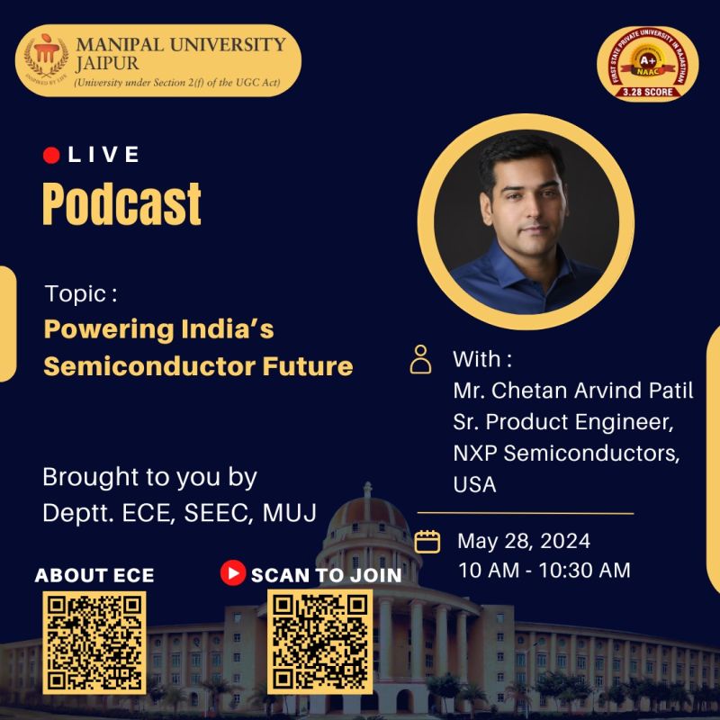
Powering India’s Semiconductor Future
- Hosted By: Manipal University Jaipur
- Location: Jaipur, Rajasthan, India (Virtual)
- Date: 27th/28th May 2024
-

The Case For Asian Semiconductor Corridor
Image Generated Using DALL-E
What Is A Semiconductor Corridor
A Semiconductor Corridor refers to a strategic network of regions and countries collaborating closely to enhance and optimize the semiconductor supply chain.
This corridor involves interconnected semiconductor manufacturing hubs, research, development, and logistics to create a more resilient and efficient semiconductor production ecosystem.
Key Components Of A Semiconductor Corridor:
By leveraging advanced manufacturing, fostering research and development, ensuring efficient supply chain integration, developing a skilled talent pool, investing in infrastructure, and implementing supportive policies, any given Semiconductor Corridor is a strategic move that aims to revolutionize the industry and secure its future for the long term.
The critical components of a Semiconductor Corridor collectively create a robust framework for advancing the global semiconductor industry. Thus, by Harnessing the specialized capabilities of different regions, such a corridor enhances technological innovation and supply chain resilience and drives economic growth and workforce development.
Component Description Manufacturing Hubs Regions within the corridor that specialize in semiconductor fabrication, assembly, testing, and packaging. These hubs leverage advanced manufacturing technologies to produce various types of semiconductor devices Research And Development Centers Institutions and facilities dedicated to the research and development of new semiconductor technologies. It includes work on advanced materials, chip designs, and innovative manufacturing processes Supply Chain Integration A streamlined and well-coordinated supply chain that ensures the efficient flow of raw materials, components, and finished products. This integration reduces delays, lowers costs, and mitigates risks associated with supply chain disruptions Talent Pool A corridor that fosters the development of skilled professionals in semiconductor technology through education, training, and workforce development programs Investment and Infrastructure Significant investments in infrastructure, including state-of-the-art manufacturing facilities, research labs, and transportation networks, to support the semiconductor industry Regulatory And Policy Support Government policies and regulations that encourage investment, innovation, and collaboration within the semiconductor sector. This includes tax incentives, research grants, and trade agreements

Picture By Chetan Arvind Patil
The Rationale For An Asian Semiconductor Corridor:
The concept of an Asian Semiconductor Corridor has emerged as a strategic response to these challenges. By leveraging the unique strengths and capabilities of Asian countries, this corridor can create a robust and integrated ecosystem that can drive innovation, enhance supply chain resilience, and foster economic growth.
The COVID-19 pandemic highlighted significant vulnerabilities in the semiconductor supply chain, demonstrating the need for a more resilient and diversified manufacturing base. An integrated corridor across Asia can mitigate these risks by ensuring a steady and reliable supply of semiconductors.
Moreover, Asia is home to some of the world’s leading semiconductor companies. The corridor can accelerate technological innovation in advanced chip design, fabrication, and packaging technologies by fostering collaboration among these entities.
Key Players In The Asian Semiconductor Corridor:
The success of the Asian Semiconductor Corridor hinges on the collaboration and contributions of key players within the region. Each country brings unique strengths and capabilities that enhance the corridor’s overall effectiveness and resilience.
Taiwan, South Korea, China, Japan, Singapore, Malaysia, Vietnam, and India each play critical roles, from advanced manufacturing and cutting-edge research to cost-effective assembly and strategic policy support.
Understanding the distinct contributions of these countries provides insight into how the Asian Semiconductor Corridor can revolutionize the global semiconductor industry.
Country Role and Contribution Taiwan As the world’s leading semiconductor manufacturer, Taiwan, with TSMC at its helm, plays a crucial role. Its expertise in advanced node fabrication is indispensable to the corridor South Korea With giants like Samsung and SK Hynix, South Korea contributes significantly in memory chips and logic devices, making it a vital player China Despite facing trade restrictions, China continues to invest heavily in its semiconductor capabilities, with SMIC leading the charge Japan Renowned for its materials and equipment, Japan’s contribution is critical in providing the necessary tools and technologies for semiconductor manufacturing Singapore A strategic hub for semiconductor manufacturing, Singapore’s established infrastructure and skilled workforce are key assets Malaysia The country’s well-established semiconductor infrastructure and industry experience make it a crucial player in this phase of the semiconductor supply chain Vietnam Similar to Malaysia, Vietnam offers cost-effective solutions for assembly and testing India With its growing focus on semiconductor design and plans to establish new fabs, India is an important player in the corridor In summary, the key players within the Asian Semiconductor Corridor form a synergistic network that drives innovation, efficiency, and growth in the semiconductor industry. By leveraging the diverse expertise and resources of Taiwan, South Korea, China, Japan, Singapore, Malaysia, Vietnam, and India, the corridor is well-positioned to address current challenges and future demands.
This collaborative effort strengthens the regional semiconductor ecosystem and enhances the global supply chain’s resilience and stability. As the corridor continues to develop, the combined strengths of these key players will be instrumental in shaping the future of semiconductor technology.
Take Away:
Establishing an Asian Semiconductor Corridor can bring a strategic initiative to harness the collective strengths of various Asian countries in the semiconductor industry. As global demand for semiconductors continues to rise, driven by technological advancements and increased digitalization, the need for a resilient and efficient supply chain has never been more critical. The Asian Semiconductor Corridor offers a comprehensive solution to address these challenges, fostering collaboration, innovation, and economic growth across the region.
In summary, the Asian Semiconductor Corridor can be a transformative initiative that promises to reshape the semiconductor landscape. It highlights the power of regional cooperation in driving technological advancements, ensuring supply chain resilience, and fostering economic growth. As the semiconductor industry continues to evolve, the corridor stands as a testament to the participating nations’ strategic foresight and collaborative spirit, paving the way for a brighter and more innovative future.
-

The Economic Edge Of Exploring The Power Of Semiconductors With Seminometrics
Image Generated Using DALL-E
Semiconductor And Economy:
The semiconductor industry is a cornerstone, powering everything from smartphones to supercomputers. As this industry further grows, understanding the economic dimensions of it becomes increasingly critical.
To capture this essence, introducing Seminometrics, an interdisciplinary field that combines the intricate technology of semiconductors with the analytical precision of econometrics.
What is Seminometrics:
Seminometrics is the fusion of semiconductor technology and econometrics. While semiconductors are the essential components in electronic devices, econometrics involves the application of statistical and mathematical methods to economic data. This innovative approach provides a comprehensive lens to examine and interpret the economic impact of semiconductors, delivering significant benefits for researchers, policymakers, and industry leaders by offering valuable insights.
Semiconductor Industry: The sector focuses on designing and manufacturing semiconductor devices like chips and transistors, essential for electronic devices
Econometrics: The application of statistical and mathematical methods to economic data to analyze and forecast economic trends
Seminometrics: An interdisciplinary field combining semiconductor technology with econometric analysis to understand and optimize the economic impact of the semiconductor industry
By combining these fields, Seminometrics aims to provide a deeper understanding of the economic dynamics driving the semiconductor industry. This includes analyzing market trends, investment strategies, production efficiencies, and the global economic impact of semiconductor advancements.
Why Understand The Economics Of Semiconductors:
Understanding the economics of semiconductors is crucial for several reasons. It drives innovation and economic growth by supporting technological advancements. Analyzing financial trends and potential returns makes informed investment decisions possible. Companies can better navigate market dynamics and consumer demands, while governments can craft effective regulations and trade policies.
Conversely, robust supply chain management ensures efficient production and risk management. Understanding labor market trends guides workforce development, and sustainability is achieved by balancing economic growth with environmental and social responsibility. By capturing all these factors, stakeholders can make informed decisions that foster a robust and sustainable semiconductor industry.

Picture By Chetan Arvind Patil
How Seminometrics Integrates Across Different Part Of Semiconductor Supply Chain:
Seminometrics, as an interdisciplinary field, integrates economic analysis across various segments of the semiconductor supply chain, providing a comprehensive understanding of the industry’s complexities and dynamics. By merging semiconductor technology with econometric methods, Seminometrics offers valuable insights into multiple critical areas:
Category Description Market Analysis The semiconductor market is highly dynamic, characterized by rapid technological advancements and shifting consumer demands. Seminometrics helps stakeholders understand these trends, enabling them to make informed decisions about product development, pricing strategies, and market positioning. Investment And Finance Investment in the semiconductor industry is crucial for innovation and growth. Seminometrics provides tools to analyze investment patterns, assess financial performance, and predict future financial trends, guiding investors and companies in optimizing their financial strategies. Production And Supply Chain Efficient production and robust supply chains are vital for the semiconductor industry. Seminometrics examines cost structures, economies of scale, and supply chain dynamics, helping companies improve production processes and manage supply chain risks effectively. Policy Impact Government policies significantly influence the semiconductor industry, from research funding to trade regulations. Seminometrics evaluates the impact of these policies, aiding policymakers in crafting regulations that foster industry growth while balancing economic and social goals. Innovation And RnD Research and development are the lifeblood of the semiconductor industry. Seminometrics measures the returns on R&D investments and their impact on industry growth, helping companies allocate resources efficiently and drive innovation. Labor Economics The semiconductor industry relies on a skilled workforce. Seminometrics analyzes employment trends, wage dynamics, and the impact of automation, providing insights into workforce development and labor market policies. Global Trade The semiconductor industry is global, with complex trade relationships. Seminometrics investigates trade flows, comparative advantages, and the impact of trade policies, offering insights into global market dynamics and trade strategy. Environmental And Social Impact As sustainability becomes a priority, Seminometrics assesses the economic impact of environmental regulations and sustainability initiatives in the semiconductor industry, balancing economic growth with social responsibility. Integrating Seminometrics across the semiconductor supply chain gives stakeholders a holistic view of market trends, investment opportunities, production efficiencies, and global trade dynamics. This interdisciplinary approach enables informed decision-making, drives innovation, and promotes sustainable economic growth.
Teaching Seminometrics In Universities:
Introducing Seminometrics as an academic discipline in universities offers students a unique and powerful framework for analyzing and optimizing the economic impact of semiconductor technologies, a skillset that is becoming more and more in demand.
By integrating principles of semiconductor science with econometric techniques, Seminometrics can equip future professionals with the knowledge and skills needed to drive innovation and sustainable growth in this critical industry.
Course Component Description Introduction To Semiconductors Cover the basics of semiconductor technology, including material science, chip design, and manufacturing processes. Principles Of Economics And Econometrics Provide a strong foundation in economics and econometrics, emphasizing data analysis, statistical methods, and economic modeling. Market Dynamics And Financial Analysis Focus on market dynamics and financial analysis specific to the semiconductor industry, using real-world case studies. Policy And Global Trade Impact Teach the impact of government policies, global trade, and international regulations on the semiconductor sector. Research And Development In Semiconductors Instruct on measuring and analyzing returns on R&D investments. Practical Applications And Case Studies Use practical applications and case studies to bridge theory and practice. Learning Seminometrics also provides students with a unique interdisciplinary skill set relevant to the modern economy. As future professionals in the semiconductor industry, students will benefit from a deep understanding of the field’s technological and economic aspects. This knowledge will enable them to make informed decisions, drive innovation, and contribute to sustainable economic growth.
Furthermore, expertise in Seminometrics will position students at the forefront of industry advancements, offering them a competitive edge in their careers and the ability to influence the future direction of semiconductor technology and its economic impact.
Take Away:
In summary, Seminometrics provides a robust framework for comprehending and harnessing the economic dynamics within the semiconductor industry. By merging the technological knowledge of semiconductor science with the analytical capabilities of econometrics, this interdisciplinary field offers critical insights that enable informed decision-making, spur innovation, and encourage sustainable economic development.
In the long term, adopting Seminometrics will keep one at the forefront of technological and economic progress in the semiconductor sector.
-

The Semiconductor Surge In India And The Impact On Other Industries
Image Generated Using DALL-E
Semiconductor And India
In recent years, the semiconductor industry has emerged as a cornerstone of modern technology, underpinning advancements in everything from consumer electronics to automotive and healthcare systems.
India, recognizing the strategic importance of this sector, has embarked on a significant push to cultivate a robust semiconductor manufacturing base.
This initiative is about augmenting India’s technological capabilities and securing its position in the global supply chain, which is crucial in a world where technological superiority increasingly dictates economic and strategic dominance.
As India accelerates its semiconductor production, understanding the broader impact of this on various domestic industries becomes essential, highlighting the interconnected nature of modern economies and the foundational role semiconductors play within them.
Semiconductor Incentives And Focus
The Indian government’s proactive measures, including substantial investments and favorable policies, are pivotal and reassuring in fostering a conducive environment for semiconductor growth. Initiatives such as the $10 billion PLI (Production-Linked Incentive) scheme aim to attract global semiconductor players and build an indigenous ecosystem supporting advanced manufacturing techniques.
This strategic development is crucial as global industries face recurrent supply chain disruptions, most notably during the COVID-19 pandemic. This underscored the vulnerability of heavy reliance on concentrated semiconductor production hubs like Taiwan and South Korea.
By establishing local manufacturing capacities, India aims to mitigate these risks and set the stage for transformative effects across multiple sectors, from telecommunications and automotive to renewable energies and beyond.
The ripple effects of enhancing semiconductor self-sufficiency are vast, warranting a thorough exploration of how this technological pivot reshapes India’s industrial landscape and its implications for future growth and innovation.

Picture By Chetan Arvind Patil
Semiconductor Impact On Other Relevant Industries In India
India’s burgeoning semiconductor industry is poised to impact various sectors, profoundly catalyzing innovation and efficiency improvements. In the automotive industry, for instance, increased local chip production ensures a steady supply of essential components for intelligent vehicles, reducing production delays and fostering advancements in vehicle safety and connectivity.
For consumer electronics, the growth of India’s semiconductor industry translates to faster production cycles and significant cost reductions. It allows manufacturers to offer competitive pricing in a price-sensitive market, reassuring the industry’s competitiveness.
The telecommunications sector benefits from enhanced capabilities in local chip production, which is crucial for supporting the expansive deployment of 5G technology and the development of robust communication networks. Additionally, renewable energy initiatives can leverage advancements in semiconductor technology to improve the efficiency and effectiveness of solar panels and energy storage systems.
Overall, the growth of India’s semiconductor industry promises to bolster the technological infrastructure, leading to a more resilient economy and stimulating innovation across diverse industrial landscapes.
Which Industries In India Will Benefit From India’s Semiconductor Manufacturing Growth
As India scales up its semiconductor production, it is essential to understand how this foundational technology will influence various domestic industries, transforming everything from automotive to agriculture through enhanced efficiency, innovation, and competitiveness.
Below is a list of key Indian industries that stand to benefit significantly from scaling up semiconductor production, along with a brief explanation of how they will be transformed.
Industry Benefits of Local Semiconductor Manufacturing Automotive Enhanced supply chain reliability for electronic components, reduced production delays, development of advanced automotive technologies like ADAS and electric vehicles Consumer Electronics Lower production costs due to localized supply chains, faster market responsiveness to consumer demands, increased competitiveness in global markets Telecommunications Support for extensive 5G rollout and infrastructure, improved manufacturing of devices like routers and modems, enhanced capabilities for IoT and smart city technologies Renewable Energy Advanced technologies for solar inverters and energy storage systems, improved grid management through sophisticated semiconductor devices, support for India’s green energy targets and sustainability initiatives Healthcare Development of more sophisticated medical devices, enhanced reliability and functionality in healthcare equipment, support for telemedicine and remote health monitoring systems Defense And Aerospace Improved supply security for critical electronic components, enhanced capabilities in surveillance, communication, and navigation systems, support for indigenous production of high-tech defense equipment Information Technology Acceleration in server and data center infrastructure development, enhanced chipsets for high-performance computing applications, support for artificial intelligence and machine learning platforms Banking And Finance Improved security and processing capabilities for financial transactions, enhanced data management and analysis for customer insights, support for fintech innovations like blockchain and cryptocurrencies Manufacturing Integration of IoT and smart factory technologies, enhanced automation and robotics driven by reliable chipsets, greater efficiency and precision in manufacturing processes Agriculture Advancements in smart agriculture technologies, enhanced capabilities for precision farming and resource management, improved IoT devices for soil, weather, and crop monitoring Take Away
As India’s semiconductor manufacturing expands, its impact on various industries will become more evident. This increased local chip production will transform sectors by enhancing supply chain resilience, fostering technological innovations, and promoting economic growth. The benefits of this surge range from more robust and efficient automotive and manufacturing sectors to more innovative and sustainable agricultural and energy practices.
The strategic improvement of semiconductor capabilities will also strengthen India’s position in the global technology arena and ensure a future where high-tech industries, innovation, and self-sufficiency support its economy. Understanding and leveraging these effects will be critical for India as it strives to become a technological powerhouse.