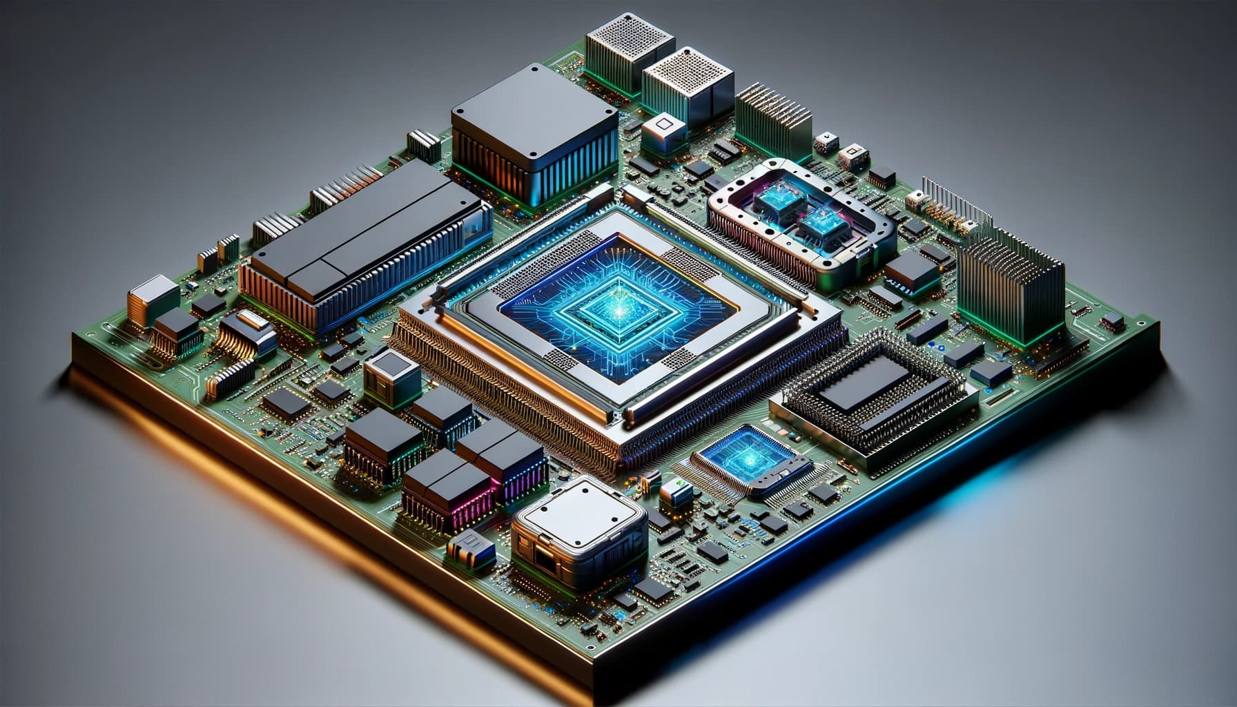
Image Generated Using DALL-E
The World Of AI SoC
Artificial Intelligence (AI) has emerged as a cornerstone in the rapidly evolving computing technology landscape, driving innovation across various sectors. At the core of AI’s transformative power are specialized silicon chips, AI Systems on Chips (SoCs), designed to process AI algorithms efficiently. These chips are pivotal in enhancing the performance and capabilities of AI applications, from autonomous vehicles and smart devices to data centers and beyond.
As AI continues to integrate into our daily lives, the companies behind these advanced SoCs play a critical role in shaping the future of technology. This list introduces the AI SoC companies taking different approaches to designing SoCs for AI applications, spotlighting their contributions to the AI revolution and their impact on the tech industry.

AI SoC Company List
Below is a work in progress, and if you find AI SoC companies that still need to be listed here, please do reach out to me.
| Company | Description |
|---|---|
| Ambarella | AI Vision Processors For Edge Applications |
| Alphawave | Provides DSP solutions for high-speed, low power consumption, enables building AISoC with AppolloCORE IP, winner of TSMC’s Awards for Excellence. |
| Anari AI | Creating cutting-edge technology to make things work in accordance with the intelligent and scalable future |
| Axelera AI | Revolutionising the field of artificial intelligence by developing a cutting-edge hardware and software platform for accelerating computer vision on edge devices |
| Axiado | To secure the end-to-end digital infrastructure by embedding a new breed of hardware-anchored AI-driven platform security in servers, 5G and network infrastructure |
| Blaize | Blaize has created a transformative new compute solution that unites silicon and software to optimize AI from the edge to the core |
| BrainChip | Specializes in developing advanced artificial intelligence and machine learning hardware |
| Celestial AI | Celestial AI is the creator of the Photonic Fabri, an optical interconnect technology platform for compute and memory |
| Cambricon Technologies | Founded in 2016, Cambrian focuses on the research and development and technological innovation of artificial intelligence chip products |
| Cerebras Systems | Uses Wafer-Scale Engine technology for deep learning, claimed to be 1000 times faster than a GPU, with innovative interconnects, memory, and package technology |
| EdgeQ | Fuses Edge and 5G into a single AI-powered chip, aiming to off-load tasks from data centers to Edge Computing |
| Enfabrica | Hardware, software, and system technologies that solve the critical bottlenecks in the next generation AI SoCs |
| Esperanto Technologies | Esperanto delivers high-performance, energy-efficient computing solutions that are the compelling choice for the most demanding AI applications |
| EnCharge AI | Leader in advanced hardware and software systems for AI computing |
| Flex Logic | Developer of embed field-programmable gate IP focused on AI SoC |
| GrAI Matter Labs | Created the fastest edge AI processor for machine vision in robotics, AR/VR, drones and more |
| Graphcore | Has built a new type of processor for machine intelligence to accelerate machine learning and AI applications for a world of intelligent machines |
| Groq | Leverages Tensor Streaming Processor (TPU) for high-speed memory and fast operations, packed in a tiny package |
| Hailo | Focuses on Edge AI, claims its Hailo processor can deliver better TOPS with high area and power efficiency |
| Horizon Robotics | Designed AI-enabled Brain Processing Units (BPU) for the automotive (Journey BPU) and IoT (Sunrise BPU) markets |
| Habana | Creates world-class AI Processors, developed from the ground-up and optimized for training deep neural networks and for inference deployment in production environments |
| Kneron | Develops an application-specific integrated circuit and software that offers artificial intelligence-based tools |
| Kinara | Kinara processors drive AI applications demanding low latency, high performance, and low power |
| LeapMind | Focuses on edge AI and machine learning |
| Lightelligence | Providing customers with powerful and effective computing power through a new paradigm of optoelectronic computing |
| Lightmatter | Chip architecture, powering faster, energy-efficient computing with photonic processors for sustainable AI advancement |
| Luminous Computing | Leverages photonics for faster AI workload training, still in stealth mode |
| Mythic AI | Utilizes Intelligence Processing Units (IPUs) for efficient, performance-oriented, cost-efficient AISoC, offers Mythic Analog Matrix Processor |
| Neureality | Developing AI inferencing accelerator chips |
| Prophesee | Uses a patented sensor design and AI algorithms that mimic the eye and brain to reveal what was invisible until now using standard frame-based technology |
| Rebellions | Develops AI accelerators by bridging the gap between underlying silicon architectures and deep learning algorithms |
| Rain Neuromorphics | Building the most energy efficient hardware for AI |
| SambaNova Systems | AI hardware and integrated systems to run AI applications from the data center to the cloud |
| SiMa.ai | Aims for greener, low-power AISoC for Edge AI, details forthcoming, plans new silicon launch |
| Synthara AG | Enables seamless integration of in-memory computing capabilities to existing chip designs, making them 130 times faster and 150 times for energy efficient |
| Syntiant | Leader in edge-AI deployments, bringing deep-learning to any device with industry-leading Neural Decision Processors and hardware-agnostic machine learning models |
| Tenstorrent | Next-generation computing company that utilizes RISC-V that builds computers for AI |
| Wave Computing | Accelerates AI computing with MIPS architecture, offers M-Class product for IoT and smart devices |
Why Care About AI SoC Companies
Understanding and keeping track of AI Systems-On-A-Chip (SoC) companies is crucial for several reasons. Firstly, these companies are at the forefront of developing the foundational technology that powers various AI applications, from consumer electronics to critical infrastructure.
Their innovations in chip design and processing capabilities directly influence the efficiency, performance, and powers of AI systems, affecting everything from energy consumption to processing speed and accuracy.
Furthermore, as AI becomes more integrated into our daily lives, these companies’ strategies and market positions have significant economic and technological implications.
By understanding the landscape of AI SoC companies, stakeholders can better navigate the technological shifts, investment opportunities, and policy considerations that shape our digital future.