- Hosted By: K. K. Wagh Institute Of Engineering Education And Research
- Location: Nashik, Maharashtra, India
- Date: 25th November 2023
Blog
-
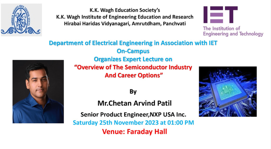
Overview of The Semiconductor Industry And Career Options
-
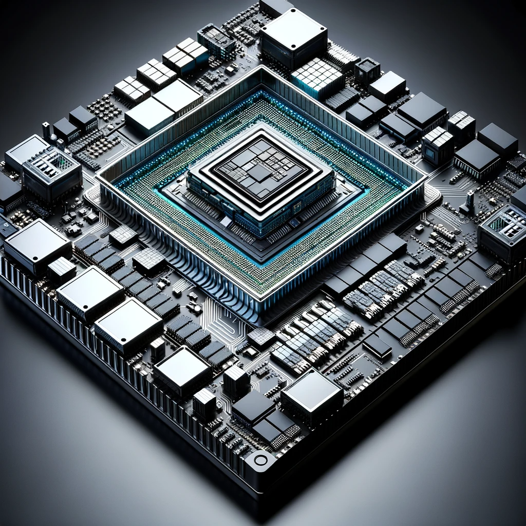
The Ways In Which OpenAI Can Reinvent Semiconductor Chip Development
Image Generated Using DALL-E
OpenAI’s involvement in semiconductor chip development could mark a significant shift in the industry, bringing about advancements in silicon design, silicon software stack development, R&D investment, and the application of GenAI in chip design.
However, the complexity and cost of chip development have escalated, posing significant challenges. It is where OpenAI, with its cutting-edge AI technologies, can play a transformative role.
Let’s explore how OpenAI can revolutionize the various aspects of semiconductor chip development.
Empowering Chip Development Teams With AI:
The first area where OpenAI can make a substantial impact is in augmenting the capabilities of chip development teams. AI models, especially those developed by OpenAI, can analyze vast amounts of data from previous chip designs, manufacturing processes, and performance metrics.
This analysis can lead to insights that would only be possible for human teams to discern due to the sheer volume and complexity of the data.
For instance, AI can predict how minor changes in the design might affect the chip’s overall performance and energy efficiency. This predictive capability can significantly reduce the time and cost of trial-and-error methods traditionally used in chip design.
Revolutionizing The Software Stack For Chip Design:
The software stack used in chip design, from schematic capture to physical layout, is ripe for innovation. OpenAI’s models can be integrated into these software tools to enhance functionality.
For example, AI can automate parts of the layout process, optimizing the placement of components to minimize signal delays and power consumption while maximizing performance.
Moreover, AI can assist in the verification process, quickly identifying potential errors or inefficiencies in the design. This integration can drastically reduce the time to market for new chips and improve their overall quality and performance.

Picture By Chetan Arvind Patil
Investing In R&D And Knowledge Building:
OpenAI’s involvement in semiconductor chip development is not just about directly applying AI technologies by building AI silicon chips but also about fostering a deeper understanding of the field.
By investing in research and development, OpenAI can help uncover new design methodologies and manufacturing techniques that could revolutionize the industry.
Furthermore, OpenAI can contribute to knowledge building around silicon chip design and manufacturing. It could involve developing AI models that simulate different manufacturing processes or predict the performance of new materials, thereby providing valuable insights to researchers and engineers.
GenAI For Silicon Chip Design:
The most futuristic application of OpenAI in chip development is the concept of Generative AI (GenAI) for silicon chip design. GenAI can go beyond optimization and generate novel chip designs based on specified parameters and performance goals.
This approach could lead to breakthroughs in chip design, uncovering configurations and architectures that humans might not conceive.
For instance, GenAI could design chips optimized explicitly for AI workloads or ultra-efficient chips for use in smart devices. The potential here is vast, and as AI technology continues to evolve, so will its chip design capabilities.
Integrating OpenAI’s technologies into semiconductor chip development heralds a new era of innovation and efficiency.
By empowering development teams, revolutionizing the silicon software stack, investing in R&D, and leveraging GenAI, OpenAI can help overcome current limitations and open up new possibilities in chip design and manufacturing.
As these technologies mature, we can expect faster, more efficient, and more powerful semiconductor chips, driving the next wave of technological advancement.
-

The Semiconductor Mobile SoC Leaders
Image Generated Using Adobe Firefly
Several companies have established themselves as prominent mobile System-On-A-Chip (SoC) technology players. The landscape is characterized by intense competition and rapid innovation, leading to the continuous evolution of SoC capabilities.
Some of the leading SoC vendors that are competing to capture a share of the mobile market are:
Qualcomm: Known for its Snapdragon series, Qualcomm is a significant player in the mobile SoC market. Its SoCs are renowned for their performance, energy efficiency, and integration of advanced features like 5G connectivity and AI capabilities.
Apple: Apple’s custom SoCs, such as the A-series used in iPhones and iPads, are highly regarded for their performance and efficiency. Apple’s control over hardware and software allows for optimized integration, resulting in impressive computational capabilities.
Samsung: Samsung Electronics, with its Exynos line of SoCs, is a key competitor in the market. These SoCs are used in various Samsung mobile devices and are known for integrating custom CPU and GPU cores.
MediaTek: MediaTek has gained significant market share, especially in the mid-range and budget segments. Its Helio and Dimensity series of SoCs balance performance and cost-effectiveness, making them popular among various smartphone manufacturers.
Huawei: Through its HiSilicon division, Huawei produces the Kirin series of SoCs. These chips are primarily used in Huawei’s range of smartphones and are known for their AI processing capabilities and 5G technology.
Google: Google has entered the SoC market with its custom Tensor chip, which powers its Pixel phones. The Tensor chip focuses on machine learning and AI tasks, leveraging Google’s expertise.
These companies have contributed to advancing mobile SoC technology through unique strengths and innovations. The choice of SoC often depends on the specific requirements of the device, including performance needs, power efficiency, connectivity options, and cost constraints.

Picture By Chetan Arvind Patil
The future of mobile SoC technology is poised for significant advancements, driven by evolving consumer demands and technological innovations. As we look toward the end, several key trends and developments are likely to shape the trajectory of mobile SoC design and capabilities:
Advanced Process Technologies: The progression towards smaller nanometer (nm) fabrication processes will continue. This evolution enables more transistors to be packed into the same space, enhancing performance and energy efficiency. Leading-edge process technologies like 3nm and beyond are to be adopted.
AI And Machine Learning: Mobile SoCs will likely see increased integration of dedicated AI and machine learning hardware. It will enhance on-device processing for image and voice recognition, augmented reality (AR) experiences, and personalized user experiences.
Next-Gen Graphic Processing: As mobile gaming and multimedia consumption grow, SoCs will integrate more powerful GPUs capable of supporting advanced graphics, high refresh rate displays, and improved AR/VR experiences.
5G And Beyond: The integration of 5G connectivity will become standard in mobile SoCs, offering faster data speeds and lower latency. Future developments may focus on optimizing 5G performance and beginning the groundwork for 6G technology.
Energy Efficiency And Battery Life: With the increasing demand for power from high-performance applications, energy efficiency remains a critical focus. Future SoCs must balance performance with power consumption to extend battery life.
Custom And Specialized SoCs: Companies may increasingly develop custom SoCs tailored to specific device needs or market segments. This trend is already visible with companies like Apple and Google developing their chips.
The future of mobile SoCs will be a blend of technological advancements and adaptations to changing user needs and global trends.
The continual push for innovation in this space suggests an exciting and dynamic future for mobile computing technology.
-
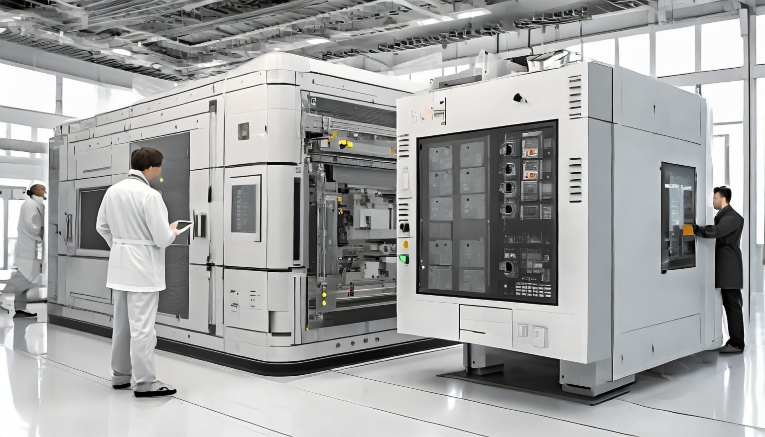
The Semiconductor Lithography Race: NIL VS EUV
Image Generated Using Adobe Firefly
In semiconductor manufacturing, lithography is a pivotal process. It involves transferring circuit patterns onto a silicon wafer, a foundational step in creating integrated circuits (ICs).
Two of the most advanced lithography techniques currently at the forefront of this industry are Extreme Ultraviolet (EUV) and Nanoimprint Lithography (NIL).
Nanoimprint Lithography (NIL) and Extreme Ultraviolet Lithography (EUV) are two technologies used in semiconductor fabrication, each with advantages and challenges. Below is a comparative analysis.
Extreme Ultraviolet Lithography (EUV):
Technical Overview: EUV lithography employs a highly sophisticated process that uses extreme ultraviolet light (with a wavelength of approximately 13.5 nm) to etch wonderful patterns onto silicon wafers. This technology is a leap from traditional lithography, which uses deep ultraviolet light.
Advantages: The primary benefit of EUV is its unparalleled resolution, allowing for the production of smaller, more complex ICs. It is crucial as the industry moves towards ever-smaller node sizes, particularly 5nm and below. EUV enables higher circuit density, contributing to the chips’ enhanced performance and energy efficiency.
Challenges And Limitations: The transition to EUV has faced significant technical and financial difficulties. The development of EUV machines, such as those produced by ASML, is incredibly costly and complex. Furthermore, EUV requires highly purified materials and controlled environments to minimize photon absorption by air or contaminants. The technology also faces throughput limitations, as EUV processes are generally slower than their deep UV counterparts.
Nanoimprint Lithography (NIL):
Technical Overview: NIL is a form of lithography that physically imprints a pattern onto a substrate using a mold or stamp. This method is similar to traditional printing techniques but at a nanometer scale.
Advantages: NIL’s main advantage lies in its simplicity and cost-effectiveness compared to EUV. It can achieve high-resolution patterns without complex light sources or optics. NIL is particularly promising for applications that require large-area patterning, such as advanced sensors and display technologies.
Challenges And Limitations: NIL’s primary challenge is defectivity and uniformity over large areas. The physical nature of the imprinting process makes it susceptible to defects caused by particle contamination or imperfections in the mold. Maintaining uniform pressure and temperature across the entire wafer during imprinting is a significant challenge.

Picture By Chetan Arvind Patil
Comparative Analysis:
Resolution And Precision: While both techniques aim to push the boundaries of miniaturization, EUV currently leads in terms of resolution and is more suited for the most advanced logic and memory devices.
Throughput And Cost: NIL offers potentially higher throughput at a lower cost, making it an attractive option for specific semiconductor applications, particularly those not requiring the extreme miniaturization capabilities of EUV.
Application Suitability: EUV is helpful for high-end, cutting-edge semiconductor fabrication, especially for CPUs and GPUs. On the other hand, NIL finds its niche in less critical layers of ICs and in specialized applications like photonics and biochips.
The race between EUV and NIL is not a straightforward competition but rather a complementarity of technologies, each serving unique semiconductor market segments. As the industry progresses, we may see advancements in both technologies, potentially leading to hybrid approaches or innovations entirely. The choice between EUV and NIL will depend on specific application requirements, cost constraints, and technological advancements.
As the semiconductor industry continues to evolve, staying abreast of these developments is crucial for manufacturers, technologists, and stakeholders in this dynamic field.
-

A Cost Analysis Of The Chiplet As A SoC Solution
Published By: Chiplet-Marketplace
Date: 9th November 2023
Media Type: Digital -

The Status Of Semiconductor Manufacturing In India
- Hosted By: MANCEF China COMET 2021
- Location: Virtual/Online
- Date: 21st – 23rd November 2021
-

Evolving Business Models of Semiconductor Design and Manufacturing
- Hosted By: Data Security Council of India
- Location: Virtual/Online
- Links: 10th November 2021
-
The Status Of Semiconductor Manufacturing In India
- Hosted By: MANCEF China COMSWORLD 2021
- Location: Virtual/Online
- Date: 16th – 17th September 2021
-

Exploration of Memory and Cluster Modes in Directory Based Many Core CMPs
- Hosted By: IEEE The International Symposium on Networks-on-Chip (NOCS)
- Location: Torino, Italy (Presented by Peers)
- Date: 4th – 5th October 2018
-

DyPO: Dynamic Pareto-Optimal Configuration Selection For Heterogeneous MpSoCs
- Hosted By: IEEE Embedded Systems Week (ESWEEK)
- Location: Seoul, South Korea (Presented by Peers)
- Date: 15th To 16th October 2017