Blog

  • The Role Of Computer Architecture In Driving Semiconductor-Powered Computing

    Image Generated Using Nano Banana


    What Computer Architecture Is And Why It Matters

    Computer architecture defines a computing system’s structure, component interaction, and trade-offs for performance, efficiency, cost, and reliability at scale. Architecture balances instruction sets, microarchitecture, memory hierarchies, and system-level design to meet workload requirements. Instruction encoding, pipeline depth, and cache topology shape both the physical silicon and the chip’s performance.

    Unlike computer organization or circuit implementation, architecture focuses on what the system does and how it exposes those capabilities to software. This includes the instruction set interface and the abstract execution model visible to compilers, operating systems, and applications.

    In semiconductor-powered computing, these architectural choices shape how transistors, the fundamental semiconductor devices, coordinate to deliver throughput, latency, efficiency, and workload specialization.

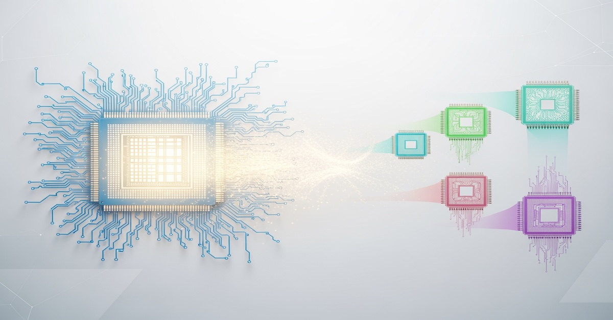
    Modern computing systems no longer rely on a single silicon engine for all performance demands. Instead, heterogeneous architectures combine general-purpose cores with specialized accelerators. This enables systems to efficiently handle workloads including sequential control logic, parallel processing, machine learning, graphics rendering, and signal processing.

    This architectural shift is a key lever for innovation as transistor scaling slows and thermal constraints tighten. By tailoring structures to specific workloads, semiconductor-powered computing continues to advance. This occurs even as raw process scaling alone becomes less effective.


    Architectural Paradigms And Workload Mapping

    As computing workloads diversified, no single architectural paradigm could efficiently meet all performance, power, and scalability demands. Computer architecture therefore evolved along multiple paths, each optimized for how computation is expressed, how data moves, and how parallelism is exploited. These paradigms are direct responses to workload characteristics such as instruction complexity, data locality, concurrency, and latency sensitivity.

    Modern systems now integrate multiple architectural paradigms within a single platform. Control-heavy functions run on general-purpose cores, while compute-dense kernels are offloaded to parallel or specialized engines. This workload-driven mapping shapes not only performance, but also silicon area allocation, power delivery, memory hierarchy, and interconnect design.

    Architectural ParadigmArchitectural FocusStrengthsBest-Suited Workloads
    General-Purpose CPU ArchitectureLow-latency execution, complex control flow, instruction-level parallelismFlexibility, strong single-thread performance, fast context switchingOperating systems, application control logic, compilation, transaction processing
    Massively Parallel ArchitectureHigh throughput via many lightweight execution unitsExcellent parallel efficiency, high arithmetic intensityGraphics rendering, scientific simulation, AI training and inference
    Vector and SIMD ArchitecturesData-level parallelism with uniform operationsEfficient execution of repetitive numeric operationsSignal processing, media processing, numerical kernels
    Domain-Specific AcceleratorsHardware optimized for narrow operation setsMaximum performance per watt for targeted tasksNeural networks, image processing, encryption, compression
    Reconfigurable ArchitecturesAdaptable hardware pipelinesFlexibility with hardware-level optimizationPrototyping, edge inference, custom data paths

    Eventually, the effectiveness of an architecture is ultimately determined by how well it matches the workload it is executing. Workloads with heavy branching and irregular memory access benefit from architectures optimized for low latency and sophisticated control logic. Highly parallel workloads with predictable data flow benefit from wide execution arrays and simplified control mechanisms. Data-intensive workloads increasingly demand architectures that minimize data movement rather than raw compute capability.


    Research Frontiers And Product Impacts

    Over the past two decades, computer architecture research has shifted from abstract performance models toward workload-driven, system-level innovation. As transistor scaling slowed and power density constraints tightened, the focus moved from peak compute capability to system interactions. Computation, memory, and data movement are now examined in real systems. Many architectural concepts shaping today’s semiconductor products started in academic research, later refined and scaled by industry.

    Heterogeneous computing is a clear example of this transition. Early research showed that offloading well-defined kernels to specialized hardware could dramatically improve performance per watt. Today, this principle underpins modern system-on-chip designs. General-purpose CPUs are now combined with GPUs and domain-specific accelerators. Apple’s silicon platforms exemplify this approach. They use tightly coupled compute engines and unified memory architectures to reduce data movement and maximize throughput.

    Image Credit: Processing-In-Memory: A Workload-Driven Perspective

    Energy efficiency has also emerged as a dominant architectural driver, particularly for data-centric workloads. Research highlighting the high energy cost of data movement has shifted architectural emphasis. Design now focuses on locality, reduced precision, and memory-centric approaches. These ideas appear in AI accelerators and data center processors. Such chips prioritize high-bandwidth memory and on-chip buffering over traditional instruction throughput.

    At the edge, research into ultra-low-power and domain-specific architectures has shaped embedded processors. These chips now achieve real-time inference and signal processing within tight energy budgets. Across all markets, architectural innovation shapes how semiconductor advances become practical computing. This trend reinforces architecture’s central role in modern systems.


    Architecture As The Linchpin Of Modern Computing

    At its core, computer architecture is the discipline that transforms raw semiconductor capability into practical, scalable computing systems. While advances in process technology determine what is physically possible, architecture determines what is achievable in real workloads. It defines how transistors are organized, how data flows through the system, and how efficiently computation is delivered under power, cost, and thermal constraints.

    As computing has expanded beyond a single dominant workload, architecture has become the critical mechanism for managing diversity. General-purpose processing, massive parallelism, and domain-specific acceleration now coexist within the same systems. Architecture governs how these elements are composed, how responsibilities are partitioned, and how bottlenecks are avoided. In doing so, it enables systems to adapt to evolving application demands without relying solely on continued transistor scaling.

    Looking ahead, the future of computing will be shaped less by uniform scaling and more by intelligent architectural design.

    Heterogeneous integration, chiplet-based systems, and workload-aware architectures will continue to define how semiconductor advances are harnessed. In this context, architecture stands as the linchpin of modern computing, holding together silicon capability, system design, and application needs into a coherent and effective whole.


  • The Semiconductor Economics Driven By Yield

    Image Generated Using Nano Banana


    Yield As The Hidden Profit Engine

    In the economics of semiconductor products, few variables exert as much influence as yield, yet few receive as little attention outside manufacturing circles. Yield quietly governs how much value can be extracted from every wafer, shaping product cost structures, margin resilience, and overall market viability.

    As devices grow more complex and manufacturing costs continue to escalate, yield increasingly acts as a hidden profit engine, amplifying gains when managed effectively and rapidly eroding profitability when overlooked.

    Yield’s impact is cumulative rather than linear. Small improvements at the wafer, assembly, or test stages compound across high-volume production, translating into meaningful reductions in cost per die and measurable gains in gross margin. From a product perspective, yield directly influences pricing strategy, supply predictability, and return on invested capital.

    Products supported by stable, high-yield manufacturing flows gain critical flexibility, whether to compete aggressively on price or to protect margins in premium markets, shaping economic outcomes long before a product reaches the customer.


    Why Yield Is Economic Leverage. Not Just a Metric

    Yield is often discussed as a manufacturing outcome and viewed primarily as an indicator of process stability, defect control, and operational discipline. While this perspective is technically valid, it significantly understates the yield’s broader economic role. It directly determines how efficiently silicon, capital equipment, energy, and engineering effort are converted into sellable product. As wafer costs rise and device complexity increases, yield becomes one of the most effective levers for influencing product cost without altering design targets or market pricing.

    Unlike many cost-reduction initiatives that require architectural trade-offs or performance compromises, yield improvements compound value throughout the entire production lifecycle. Higher yield increases usable output per wafer, stabilizes manufacturing schedules, and reduces losses from scrap, rework, and late-stage failures. From a product and business standpoint, yield therefore functions as economic leverage rather than a passive metric, shaping profitability, pricing flexibility, and capital efficiency simultaneously.

    DimensionYield Viewed as a MetricYield Viewed as Economic Leverage
    Primary FocusProcess health and defect levelsProduct cost, margin, and profitability
    ScopeIndividual manufacturing stepsEnd to end product economics
    Impact HorizonShort term manufacturing performanceLong term financial and competitive outcomes
    Cost InfluenceIndicates loss but does not control itActively reduces cost per die
    Capital EfficiencyMeasured after investmentGuides investment justification and ROI
    Product StrategyReactive inputProactive decision driver
    Business VisibilityLimited to manufacturing teamsRelevant to product, finance, and leadership

    As semiconductor products move toward advanced nodes, heterogeneous integration, and increasingly complex test and packaging flows, the economic sensitivity to yield will only intensify.

    Companies that elevate yield from a manufacturing statistic to a strategic economic variable will be better positioned to protect margins, sustain innovation, and compete effectively in cost-constrained and performance-driven markets.


    Yield’s Impact On Product Economics

    From a product perspective, yield influences economics at every stage of the lifecycle. During early ramps, unstable yields inflate unit costs and delay break-even points. In high-volume production, sustained yield performance protects gross margins and reduces exposure to cost shocks from scrap, rework, or supply disruptions.

    Products manufactured on mature, high-yield processes gain economic resilience, while those burdened by yield variability often require pricing premiums or volume constraints to remain profitable.

    Economic DimensionRole of YieldProduct Level Impact
    Cost Per DieDetermines usable output per waferLower yield increases unit cost and reduces competitiveness
    Gross MarginExpands sellable volume without increasing wafer startsHigher yield improves margin resilience
    Pricing StrategyEnables flexibility between margin protection and market shareStable yield supports aggressive or premium pricing
    Time to MarketReduces rework and ramp delaysFaster revenue realization
    Capital EfficiencyImproves return on fab and equipment investmentHigher ROI on advanced nodes
    Supply PredictabilityStabilizes output forecastsStronger customer commitments and fewer shortages

    Eventually, yield is not merely a manufacturing outcome. It is a core economic variable that defines how effectively a semiconductor product converts technical capability into financial return.

    Products with strong yield performance gain pricing power, margin stability, and supply reliability, all of which are critical in competitive, cost-sensitive markets.

    As semiconductor products continue to grow in complexity and cost, yield will increasingly determine who wins and loses economically.

    Organizations that integrate yield considerations into product planning, financial modeling, and strategic decision making will be better positioned to deliver profitable, scalable, and resilient semiconductor products.


  • The Semiconductor Shift Toward Processor-In-Memory And Processing-Near-Memory

    Image Generated Using Nano Banana


    Reliance Of AI And Data Workloads On Computer Architecture

    AI and modern data workloads have transformed how we think about computing systems. Traditional processors were designed for sequential tasks and moderate data movement. Today’s AI models work with enormous datasets and large numbers of parameters that must move constantly between memory and compute units. This movement introduces delays and consumes significant energy. As a result, memory bandwidth and the distance to the data have become major performance bottlenecks.

    Graphics processors, tensor accelerators, and custom architectures try to address these issues by increasing parallelism. Yet, parallel computing alone cannot solve the challenge if data cannot reach the compute units fast enough. The cost of moving data inside a system is now often higher than the cost of the computation itself.

    This places the spotlight on the relationship between compute location, memory hierarchy, and data flow. As models grow in size and applications demand faster responses, the gap between processor speed and memory access continues to widen.

    The computing industry often refers to this as the memory wall. When AI tasks require moving gigabytes of data per operation, each additional millimeter of distance within a chip or package matters. To break this pattern, new approaches look at placing compute engines closer to where data is stored.

    This shift has sparked interest in Processor In-Memory and Processing Near-Memory solutions.

    Instead of pulling data along long paths, the system reorganizes itself so that computation occurs either within the memory arrays or very close to them. This architectural change aims to reduce latency, cut energy use, and support the growing scale of AI workloads.


    What Is Processor-In-Memory And Processing-Near-Memory

    Processor-In-Memory places simple compute units directly inside memory arrays. The idea is to perform certain operations, such as multiplication and accumulation, inside the storage cells or peripheral logic. By doing this, data does not need to travel to a separate processor. This can lead to significant improvements in throughput and reductions in energy consumption for specific AI tasks, especially those involving matrix operations.

    Processing-Near-Memory keeps memory arrays unchanged but integrates compute units very close to them, usually on the same stack or interposer. These compute units are not inside the memory but sit at a minimal distance from it. This enables faster data access than traditional architectures without requiring significant changes to memory cell structures. PNM often offers a more flexible design path because memory vendors do not need to modify core-array technology.

    Here is a simple comparison of the two approaches.

    FeatureProcessor-In-MemoryProcessing-Near-Memory
    Compute locationInside memory arrays or peripheral logicAdjacent to memory through same stack or substrate
    Memory modificationRequires changes to memory cell or array designUses standard memory with added compute units nearby
    Data movementVery low due to in-array operationLow because compute is positioned close to data
    FlexibilityLimited to specific operations built into memoryWider range of compute tasks possible
    Technology maturityStill emerging and specializedMore compatible with existing memory roadmaps

    Both approaches challenge the long-standing separation between computing and storage. Instead of treating memory as a passive container for data, they treat it as an active part of the computation pipeline. This helps systems scale with the rising demands of AI without relying entirely on larger, more power-hungry processors.


    Research Efforts For Processor In Memory And Processing Near Memory

    Research activity in this area has grown quickly as AI and data workloads demand new architectural ideas. Both Processor In Memory and Processing Near Memory have attracted intense attention from academic and industrial groups. PIM work often focuses on reducing data movement by performing arithmetic inside or at the edge of memory arrays. At the same time, PNM research explores programmable compute units placed near memory stacks to improve bandwidth and latency.

    The selected examples below show how each direction is pushing the boundaries of energy efficiency, scalability, and workload suitability.

    Image Credit: SparseP
    CategoryExample WorkKey FocusWhat It DemonstratesLink
    Processor In MemorySparseP: Efficient Sparse Matrix Vector Multiplication on Real PIM Systems (2022)Implements SpMV on real PIM hardwareShows strong gains for memory-bound workloads by computing inside memory arraysPaper
    Processor In MemoryNeural-PIM: Efficient PIM with Neural Approximation of Peripherals (2022)Uses RRAM crossbars and approximation circuitsShows how analog compute in memory can accelerate neural networks while cutting conversion overheadPaper
    Processing Near MemoryA Modern Primer on Processing In Memory (Conceptual framework)Defines PIM vs PNM in stacked memory systemsClarifies architectural boundaries and highlights PNM integration paths in 3D memoryPaper
    Processing Near MemoryAnalysis of Real Processing In Memory Hardware (2021)Evaluates DRAM with adjacent compute coresProvides methods used widely in PNM evaluation for bandwidth and workload behaviorPaper

    This comparison above captures both experimental implementations and architectural frameworks.

    Together, they show how PIM pushes compute directly into memory structures, while PNM enables more flexible acceleration by placing logic close to high-bandwidth memory.


    Implications And When Each Approach Can Benefit

    Processor-In-Memory is often most useful when the workload is highly repetitive and dominated by simple arithmetic on large matrices. Examples include neural network inference and certain scientific operations. Since operations occur in memory, energy savings can be substantial. However, PIM is less suitable for general-purpose tasks that require flexible instruction sets or complex branching.

    Processing-Near-Memory is a more adaptable option for systems that need performance improvements but cannot redesign memory cells. It supports tasks such as training large AI models, running recommendation engines, and accelerating analytics pipelines. Because PNM units are programmable, they can handle a broader range of workloads while still providing shorter data paths than traditional processors.

    Image Credit: Computing Landscape Review

    In real systems, both approaches may coexist. PIM might handle dense linear algebra while PNM handles control logic, preprocessing, and other mixed operations. The choice depends on workload structure, system integration limits, and power budgets. As AI becomes embedded in more devices, from data centers to edge sensors, these hybrids create new ways to deliver faster responses at lower energy.


    The Direction Forward

    The movement toward Processor-In-Memory and Processing-Near-Memory signals a larger architectural shift across the semiconductor world. Instead of treating compute and memory as separate units connected by wide interfaces, the industry is exploring tightly coupled designs that reflect the actual behavior of modern AI workloads. This shift helps push past the limits of conventional architectures and opens new opportunities for performance scaling.

    As more applications rely on real-time analytics, foundation models, and data-intensive tasks, the pressure on memory systems will continue to increase. Designs that bring compute closer to data are becoming essential to maintaining progress. Whether through in-memory operations or near-memory acceleration, these ideas point toward a future where data movement becomes a manageable cost rather than a fundamental barrier.

    The direction is clear. To support the next generation of AI and computing systems, the computing industry is rethinking distance, energy, and data flow at the chip level. Processor-In-Memory and Processing-Near-Memory represent two critical steps in that journey, reshaping how systems are built and how performance is achieved.


  • AI-Driven Semiconductor Solutions

    • Panel Moderator
    • Hosted By: The IEEE Future Tech Forum Panel As Part Of IEEE Global Semiconductors Initiative Under IEEE Future Directions.
    • Location: Virtual/Online
    • Date: 18th December 2025

  • The Expanding Scale of Semiconductor Test Data

    Published By: Electronics Product Design And Test
    Date: December 2025
    Media Type: Online Media Website And Digital Magazine

  • The Semiconductor Productivity Gap And Why It Matters

    Image Generated Using Nano Banana


    The Shifting Foundations Of Semiconductor Productivity

    Productivity in semiconductors was once anchored in a predictable formula in which each new node delivered higher transistor density, better performance per watt, and stable cost per transistor. That engine is weakening.

    Design complexity has surged, stretching development cycles from roughly 6-12 months to 12-24 months or more for leading-edge SoCs, driven by more than 1.5 billion verification cycles and verification workloads that account for 55 percent of total effort.

    Manufacturing is under similar strain, as EUV tools consume nearly 1 megawatt per scanner, require over 50% uptime for economic breakeven, and demand more than planned service interventions per year. Costs per reticle, mask, and process layer continue to rise, breaking the traditional assumption that fabs scale efficiently through capital expansion.

    Talent constraints further intensify the challenge. Deloitte’s Semiconductor Workforce Study forecasts a shortage of more than 1 million skilled workers by 2030, with acute gaps in RF, physical, lithography, and packaging. Many of these jobs require 3 to 5 years of training before reaching full productivity, meaning that new fabs deliver immediate capital capacity but delayed human-capacity scaling.

    As complexity, cost, and workforce requirements outpace traditional efficiency levers, the industry faces a widening productivity gap reflected in slower node adoption, rising unit costs, and delayed revenue realization. Closing this gap requires a fundamental rethinking of design automation, manufacturing operations, and the leverage of engineering.


    Why The Productivity Gap Matters For The Global Semiconductor Business

    The productivity gap has significant economic consequences across the semiconductor value chain. Time-to-market pressure is among the most critical. As semiconductor delivery timelines stretch, downstream industries slow correspondingly, creating friction across entire product ecosystems.

    Capital efficiency is also under strain. A modern 5 nm fab requires more than $ 20 billion in investment, yet wafer starts per tool are growing more slowly than capital intensity. SEMI’s 2024 World Fab Forecast reports that leading-edge capacity grew only 6 percent in 2023 while capital intensity rose nearly 12 percent, meaning each incremental wafer requires disproportionately higher investment.

    Combined with slowing node transitions and reduced cost-per-transistor improvements, the traditional economic benefits of scaling are diminishing. This puts pressure on business models that depend on rapid node migration, especially in high-volume mobile and compute markets.

    These effects cascade across supply chains: delayed design inputs slow fab loading, manufacturing bottlenecks delay customer shipments, and product cycles across electronics, automotive, cloud, and AI sectors lose momentum.

    The semiconductor productivity gap, therefore, acts as a drag on global innovation, competitiveness, and economic growth.


    How AI And Automation Can Close The Semiconductor Productivity Gap

    Artificial intelligence and automation are emerging as the most powerful tools to bridge the productivity divide. The goal is not only faster execution but also more thoughtful execution. AI has the potential to collapse design loops, optimize fab operations, and augment the limited engineering workforce.

    In design, AI-driven EDA tools can accelerate RTL generation, automate physical design exploration, and reduce verification workloads. Google’s reinforcement learning floorplanner demonstrated a 10x reduction in layout search time in published results from Nature. AI-based verification triage systems can analyze failing regressions and automatically cluster root causes, reducing engineering debug by hours.

    In manufacturing, AI-enabled process control can stabilize fabs with fewer interventions. Predictive maintenance models for etch and deposition tools can extend mean time between failures, and when fab equipment availability increases, overall fab productivity rises without proportional increases in labor or capital.

    AreaPossible AI TechniqueImpact
    RTL to GDS designGenerative RTL and automated floorplanningFaster architecture exploration and reduced layout search time
    VerificationRegression clustering and failure triageSignificant reduction in debug workload
    LithographyDose and focus machine learning correctionLower variation and fewer rework cycles
    Fab equipmentPredictive maintenance using MLExtended mean time between failures and higher uptime
    Supply chainAI-based demand and risk forecastingImproved continuity and reduced inventory exposure

    The combined effect of these improvements is significant. Even moderate efficiency gains across thousands of design engineers or hundreds of fab tools produce measurable bottom-line impact. AI gives the industry new scaling levers at a time when traditional scaling is slowing.


    Strategic Imperatives For A More Productive Semiconductor Future

    The semiconductor productivity gap is real, expanding, and rooted in structural forces that will not correct on their own. Rapid growth in design complexity, mounting manufacturing challenges, and a global shortage of skilled engineers are stretching development cycles and reducing the economic leverage the industry once relied on.

    These pressures slow innovation, raise costs, and weaken the longstanding assumption that each new node or product generation will automatically deliver meaningful productivity gains.

    Addressing this gap requires coordinated action across technology, workforce, and capital strategy. AI and automation provide the most powerful levers, with the potential to create new productivity curves similar to the early years of EDA and factory automation.

    Companies that embed AI-driven workflows throughout design and manufacturing will move faster, utilize capital more efficiently, and operate more resilient supply chains. By modernizing workflows and strengthening engineering leverage, the industry can rebuild the compounding productivity that once defined semiconductor progress and support the next decade of global technological growth.


  • The Rise Of Semiconductor Agents

    Image Generated Using Nano Banana


    What Are Semiconductor Agents

    Semiconductor Agents are AI model-driven assistants built to support the digital stages of chip development across design, verification, optimization, and analysis. Unlike traditional automation scripts or rule-based flows, these agents use large models trained on RTL, constraints, waveforms, logs, and tool interactions.

    This gives them the ability to interpret engineering intent, reason about complex design states, and take autonomous actions across EDA workflows. In practical terms, they act as specialized digital coworkers that help engineers manage work that is too large, too repetitive, or too interconnected for manual execution.

    In design, these agents can generate RTL scaffolds, build verification environments, explore architectural tradeoffs, analyze regression failures, and recommend PPA improvements. In verification, they generate tests, identify coverage gaps, diagnose failure signatures, and run multi-step debug sequences. In physical design, they assist with constraint tuning, congestion analysis, timing closure, and design space exploration by using model-driven reasoning to evaluate large option spaces much faster than human iteration.

    Put simply, model-driven semiconductor agents are intelligent systems that accelerate, improve accuracy, and scale chip development. They convert slow, script-heavy engineering loops into guided, automated workflows, representing a significant shift in how modern silicon will be created.


    Are These Agents Real Or Hype?

    Model-driven semiconductor agents are no longer a future idea. They are already used in modern EDA platforms, where they automate tasks such as RTL generation, testbench creation, debug assistance, and design optimization.

    These agents rely on large models trained on engineering data, tool interactions, and prior design patterns, which allows them to operate with a level of reasoning that simple scripts cannot match.

    Academic research supports this progress. For example, one paper (“Proof2Silicon: Prompt Repair for Verified Code and Hardware Generation via Reinforcement Learning”) reports that using a reinforcement-learning guided prompt system improved formal verification success rates by up to 21% and achieved an end-to-end hardware synthesis success rate of 72%.

    another study (“ASIC‑Agent: An Autonomous Multi‑Agent System for ASIC Design with Benchmark Evaluation”) the authors introduce a sandboxed agent architecture that spans RTL generation, verification, and chip integration, demonstrating meaningful workflow acceleration.

    These research-driven examples show that model-driven and agent-based methods are moving beyond concept toward applied results in chip design.

    It is still early, and no single agent can design a full chip. Human engineers guide decisions, verify results, and manage architectural intent. But the momentum is real. Model-driven semiconductor agents are practical, maturing quickly, and steadily becoming an essential part of how the industry will design and verify chips at scale.


    How Semiconductor Agents Integrate Into the Silicon Lifecycle

    In early design exploration, a semiconductor agent could take a natural-language module description and generate an initial RTL draft along with interface definitions and bare assertions. Engineers would then refine the output instead of starting from a blank file. This reduces time spent on boilerplate RTL and allows teams to explore architectural directions more quickly and with less friction.

    During verification, an agent could analyze regression results, classify failures based on patterns in signals and logs, and propose a minimal reproduction test. This turns hours of manual waveform inspection into a short, actionable summary. Engineers receive clear guidance on where a failure originated and why it may be happening, which shortens debug cycles and helps verification progress more consistently.

    Stage of LifecyclePossible Agent Use CaseWhat The Agent Can DoValue to Engineering Teams
    DesignRTL Draft GenerationConverts written specifications into initial RTL scaffolds and interface definitionsFaster architecture exploration and reduced boilerplate coding
    DesignConstraint & Architecture SuggestionsAnalyzes goals and proposes timing, power, or area tradeoff optionsHelps evaluate design alternatives quickly
    VerificationAutomated Testbench GenerationBuilds UVM components, assertions, and directed tests from module descriptionsReduces manual setup time and accelerates early verification
    VerificationRegression Triage & Pattern DetectionClassifies failures, identifies recurring issues, and recommends likely root causesCompresses debug cycles and improves coverage closure
    Physical DesignPPA ExplorationEvaluates multiple constraint and floorplan options using model reasoningNarrows the search space and speeds up timing closure
    Physical DesignCongestion & Timing AnalysisPredicts hotspots or slack bottlenecks and suggests candidate fixesReduces the number of full P&R iterations
    SignoffIntelligent Rule CheckingIdentifies high-risk areas in timing, IR drop, or design-for-test based on learned patternsHelps engineers prioritize review efforts
    Product EngineeringAnomaly Detection in Pre-Silicon DataAnalyzes logs, waveform summaries, or DFT patterns to detect inconsistenciesImproves first-silicon success probability
    System Bring-UpIssue LocalizationInterprets bring-up logs and suggests potential firmware or hardware mismatchesShortens early debug during lab validation

    In physical design, an agent could evaluate many constraints and floorplan variations using model-driven reasoning. By analyzing congestion signatures, timing slack, and area tradeoffs, it could narrow the design space to a few strong candidates. Engineers would then focus on validating these options rather than manually exploring hundreds of combinations, thereby improving both the speed and the quality of timing closure.


    Who Is Building Semiconductor Agents And What It Takes

    EDA vendors and a new generation of AI-EDA startups are primarily developing semiconductor agents. Established tool providers are adding large models into their design and verification platforms, while startups are building agent-first workflows for RTL, verification, and debug. These systems sit on top of existing EDA engines and aim to reduce repetitive engineering work.

    Building these agents requires deep domain data and strong tool integration. Helpful agents depend on RTL datasets, constraints, logs, waveforms, and optimization traces. They also need alignment layers that help the model understand engineering intent and connect reliably to commercial EDA tools, enabling execution of multi-step flows.

    CategoryWho Is Building ThemWhat They ContributeWhat It Takes to Build Agents
    EDA VendorsEstablished design-tool providersAgent-assisted RTL, verification, debugLarge datasets, tight EDA integration, safety guardrails
    AI-EDA StartupsModel-focused EDA companiesMulti-agent workflows and rapid innovationProprietary models and close customer iteration
    Semiconductor CompaniesInternal CAD and design teamsReal data and domain expertiseAccess to RTL, ECO histories, regressions, waveforms
    Academic LabsUniversities and research centersNew multi-agent methods and algorithmsResearch datasets and algorithm development

    Trust and correctness are central to building these agents. Because chip design errors are costly, teams need guardrails, human oversight, and verifiable outputs. Agents must behave predictably and avoid changes that violate timing, physical, or functional rules.

    In summary, semiconductor agents are being built by organizations with the correct data, EDA expertise, and safety practices. Creating them requires large models, strong domain alignment, and deep integration with existing tools, and these foundations are now driving their rapid adoption.


  • The Expanding Scale of Semiconductor Test Data

    Published By: Electronics Product Design And Test
    Date: November 2025
    Media Type: Online Media Website And Digital Magazine

  • The Semiconductor Compute Shift From General-Purpose To Purpose-Specific

    Image Generated Using Nano Banana


    The End Of Architectural Consensus

    The semiconductor industry is undergoing a fundamental architectural break. For over 50 years, general-purpose computing has prevailed thanks to software portability, transistor-driven scaling, and the absence of workloads that demanded radical alternatives. That era is over.

    With Moore’s Law slowing to single-digit gains and Dennard scaling effectively dead, the hidden energy and performance subsidy that made CPUs “good enough” has vanished. Meanwhile, AI workloads now require 100x to 10,000x more compute than CPUs can provide economically, forcing a shift to purpose-built architectures.

    What has changed is not that specialized processors are faster, which has always been true, but that the performance gap is now so large it justifies ecosystem fragmentation and platform switching costs.

    Specialized architectures win because their optimizations compound. They align parallelism with workload structure, tune memory access patterns, scale precision to algorithmic tolerance, and embed domain-specific operations directly in hardware.

    These advantages multiply into 10,000x efficiency improvements that approach thermodynamic limits. General-purpose chips cannot close that gap, regardless of how many transistors they add.


    Vertical Integration For Purpose-Specific Silicon Design

    The shift toward custom silicon marks one of the most consequential strategic pivots in modern computing. For decades, the industry relied on merchant silicon vendors to supply general-purpose processors, enabling broad ecosystem access and a relatively level competitive field. That balance is now collapsing.

    When companies like Google, Amazon, and Meta invest billions to design their own chips, once the domain of specialized semiconductor vendors, they are not simply optimizing compute units. They are vertically integrating the computational stack.

    The table below describes the mechanism and path by which vertical integration in silicon is leading to the reconcentration of computing power:

    PhaseCompute Architecture ModelSilicon StrategyCore Capability RequirementsWhere Value Is CapturedIndustry Structure
    Phase 1General Purpose ComputingMerchant siliconProcurement, standardization, software portabilityChip vendors, CPU platformsBroad, horizontal, open ecosystem
    Phase 2Accelerated Computing (GPU era)Domain-optimized acceleratorsParallel programming models, runtime frameworksSilicon + software stacksEarly signs of consolidation
    Phase 3AI-Native Compute PlatformsLight customization, firmware-level tuningPackaging, interconnect tuning, software toolchainsSilicon + compiler + runtimeCompute access becomes bottleneck
    Phase 4Vertically Integrated ComputeIn-house or deeply co-designed acceleratorsArchitecture, EDA, compiler, systems designSilicon + system + cloud economicsAdvantage shifts to those controlling full stack
    Phase 5Silicon-Native InfrastructureFull-stack co-optimization: chip, system, workloadAlgorithm + hardware co-design, multi-year roadmapsEnd-to-end platform controlReconcentration, winner-take-most dynamics

    The economic logic is clear: even small efficiency gains, measured in single-digit percentage improvements, translate into hundreds of millions in savings when spread across millions of processors and tens of thousands of AI clusters.

    At the same time, custom silicon enables performance and efficiency profiles that off-the-shelf solutions cannot match. The result is not just faster chips, but the ability to architect entire data centers, scheduling systems, memory fabrics, and cooling environments around silicon they control years in advance.


    Components of An AI Server | Image Credit: Mckinsey & Company

    The Two-Tier Computing Economy And Consequences

    A structural divide has emerged in modern computing, characterized by a two-tier computing economy, where traditional workloads continue to run efficiently on commodity CPUs. At the same time, AI and frontier applications require specialized accelerators that general-purpose processors cannot support.

    This split mirrors the evolution of high-performance computing, where systems like Frontier had no choice but to adopt thousands of GPU accelerators to reach exascale within power and cost constraints.

    The same dynamic now extends beyond HPC. Apple Silicon demonstrates how custom chips deliver performance-per-watt advantages that are impossible with merchant x86 processors, while Tesla’s autonomous driving processors show that real-time AI inference under tight thermal limits demands entirely new silicon architectures.

    The consequence is a computing landscape divided by capability, economics, and accessibility. Those with the scale, capital, and technical depth to design or co-design silicon gain access to performance and efficiency unattainable through merchant hardware.

    Everyone else must either rent access to specialized accelerators through hyperscalers, creating a structural dependency, or remain constrained to slower, less efficient CPU-based systems.

    In effect, computing is entering a new era where advanced capabilities are increasingly concentrated, echoing the mainframe era but now driven by AI, thermodynamics, and silicon control at a planetary scale.


    Image Credit: Mckinsey & Company

    Strategic Implications And The Post-General-Purpose Landscape

    As computing splinters into purpose-specific architectures, the tradeoff between optimization and portability becomes unavoidable. The collapse of the “write once, run anywhere” model forces developers to choose between sacrificing up to 30 to 90 percent of potential performance on general-purpose hardware or investing in architecture-specific optimization that fragments codebases.

    In AI alone, models running unoptimized on CPUs can perform 50 to 200 times slower than on accelerators designed for tensor operations. Every new accelerator also demands its own toolchains, compilers, profilers, and programming abstractions. This is why companies now spend more on their AI engineering effort adapting models to specific silicon targets, rather than improving the models themselves.

    The economics create a structural divide. Custom silicon becomes cost-effective only at a massive scale, typically involving one to three million deployed processors, or under extreme performance constraints such as autonomous driving or frontier AI training. Below that threshold, organizations must rely on cloud accelerators, locking them into hyperscaler pricing and roadmaps. The strategic dimension is equally clear.

    Control over custom silicon provides supply security and technology sovereignty, especially as export controls and geopolitical friction reshape semiconductor access. The result is a rapidly diverging compute landscape. Innovation accelerates as specialized architectures explore design spaces that general-purpose CPUs never could.

    Still, the cost is a fragmented ecosystem and a concentration of computational power among those with the scale, capital, and silicon capability to shape the post-general-purpose era.


  • The Case For Building AI Stack Value With Semiconductors

    Image Generated Using DALL·E


    The Layered AI Stack And The Semiconductor Roots

    Artificial intelligence operates through a hierarchy of interdependent layers, each transforming data into decisions. From the underlying silicon to the visible applications, every tier depends on semiconductor capability to function efficiently and scale economically.

    The AI stack can be imagined as a living structure built on four essential layers: silicon, system, software, and service.

    Each layer has its own responsibilities but remains fundamentally connected to the performance and evolution of the chips that power it. Together, these layers convert raw computational potential into intelligent outcomes.

    At the foundation lies the silicon layer, where transistor innovation determines how many computations can be executed per joule of energy. Modern nodes, such as those at 5 nm and 3 nm, make it possible to create dense logic blocks, high-speed caches, and finely tuned interconnects that form the core of AI compute power.

    AI Stack LayerExample TechnologiesSemiconductor Dependence
    SiliconLogic, memory, interconnectsDetermines compute density, power efficiency, and speed
    SystemBoards, servers, acceleratorsDefines communication bandwidth, cooling, and energy distribution
    SoftwareFrameworks, compilers, driversConverts algorithmic intent into hardware-efficient execution
    ServiceCloud platforms, edge inference, APIsScales models to users with predictable latency and cost

    Above this, the system layer integrates the silicon into servers, data centers, and embedded platforms. Thermal design, packaging methods, and signal integrity influence whether the theoretical performance of a chip can be achieved in real-world operation.

    Once silicon is shaped into functional systems, software becomes the crucial bridge between mathematical models and physical hardware. Frameworks such as TensorFlow and PyTorch rely on compilers like XLA and Triton to organize operations efficiently across GPUs, CPUs, or dedicated accelerators. When these compilers are tuned to the architecture of a given chip, its cache size, tensor core structure, or memory hierarchy, the resulting improvements in throughput can reach 30-50 percent.

    At the top of the stack, the service layer turns computation into practical value. Cloud APIs, edge inference platforms, and on-device AI engines rely on lower layers to deliver low-latency responses at a global scale. Even a modest reduction in chip power consumption, around ten percent, can translate into millions of dollars in savings each year when replicated across thousands of servers.

    In essence, the AI stack is a continuum that begins with electrons moving through transistors and ends with intelligent experiences delivered to users. Every layer builds upon the one below it, transforming semiconductor progress into the computational intelligence that defines modern technology.


    Image Credit: The 2025 AI Index Report Stanford HAI

    AI Value From Transistors To Training Efficiency

    The value of artificial intelligence is now measured as much in terms of energy and computational efficiency as in accuracy or scale. Every improvement in transistor design directly translates into faster model training, higher throughput, and lower cost per operation. As process nodes shrink, the same watt of power can perform exponentially more computations, reshaping the economics of AI infrastructure.

    Modern supercomputers combine advanced semiconductors with optimized system design to deliver performance that was previously unimaginable.

    The table below illustrates how leading AI deployments in 2025 integrate these semiconductor gains, showing the connection between chip architecture, energy efficiency, and total compute output.

    AI Supercomputer / ProjectCompany / OwnerChip TypeProcess NodeChip QuantityPeak Compute (FLOP/s)
    OpenAI / Microsoft – Mt Pleasant Phase 2OpenAI / MicrosoftNVIDIA GB2005 nm700 0005.0 × 10¹⁵
    xAI Colossus 2 – Memphis Phase 2xAINVIDIA GB2005 nm330 0005.0 × 10¹⁵
    Meta Prometheus – New AlbanyMeta AINVIDIA GB2005 nm300 0005.0 × 10¹⁵
    Fluidstack France Gigawatt CampusFluidstackNVIDIA GB2005 nm500 0005.0 × 10¹⁵
    Reliance Industries SupercomputerReliance IndustriesNVIDIA GB2005 nm450 0005.0 × 10¹⁵
    OpenAI Stargate – Oracle OCI ClusterOracle / OpenAINVIDIA GB3003 nm200 0011.5 × 10¹⁶
    OpenAI / Microsoft – AtlantaOpenAI / MicrosoftNVIDIA B2004 nm300 0009.0 × 10¹⁵
    Google TPU v7 Ironwood ClusterGoogle DeepMind / Google CloudGoogle TPU v74 nm250 0002.3 × 10¹⁵
    Project Rainier – AWSAmazon AWSAmazon Trainium 27 nm400 0006.7 × 10¹⁴
    Data Source: Epoch AI (2025) and ML Hardware Public Dataset

    From these figures, it becomes clear that transistor scaling and system integration jointly determine the value of AI. Each new semiconductor generation improves energy efficiency by roughly forty percent, yet the total efficiency of a supercomputer depends on how well chips, networks, and cooling systems are co-optimized.

    The GB300 and B200 clusters, built on advanced 3nm and 4nm processes, deliver near-exponential performance per watt compared to earlier architectures. Meanwhile, devices such as Amazon Trainium 2, based on a mature 7nm node, sustain cost-effective inference across massive cloud deployments.

    Together, these systems illustrate that the future of artificial intelligence will be shaped as much by the progress of semiconductors as by breakthroughs in algorithms. From mature 7 nm inference chips to advanced 3 nm training processors, every generation of silicon adds new layers of efficiency, capability, and intelligence.

    As transistors continue to shrink and architectures grow more specialized, AI value will increasingly be defined by how effectively hardware and design converge. In that sense, the story of AI is ultimately the story of the silicon that powers it.