Blog

  • The Semiconductor Technology Node India Should Focus On

    Photo by Maxence Pira on Unsplash


    India is betting on end-to-end semiconductor manufacturing, which is the right step to meet the growing demand for the country’s semiconductor requirements. If executed as planned, the import of silicon chips will drastically decrease and will remove the dependency on the other countries.

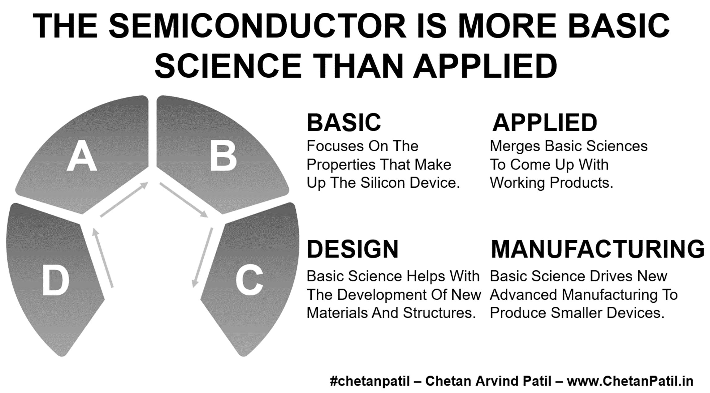
    The technology node is crucial to getting the semiconductor manufacturing strategy correct. It is at the core of any silicon chip that ever gets produced, and for a country like India, where the majority of the semiconductor manufacturing (mainly the FAB/fabrication part) is confined to public units and caters to the country’s space, defense, and other critical national infrastructure needs. Leveraging these foundations and extending the technology node capabilities to develop more India-centric process technologies is more beneficial.

    The Technology Node (Also Process Node, Process Technology, Or Simply Node) Refers To A Specific Semiconductor Manufacturing Process And Its Design Rules.

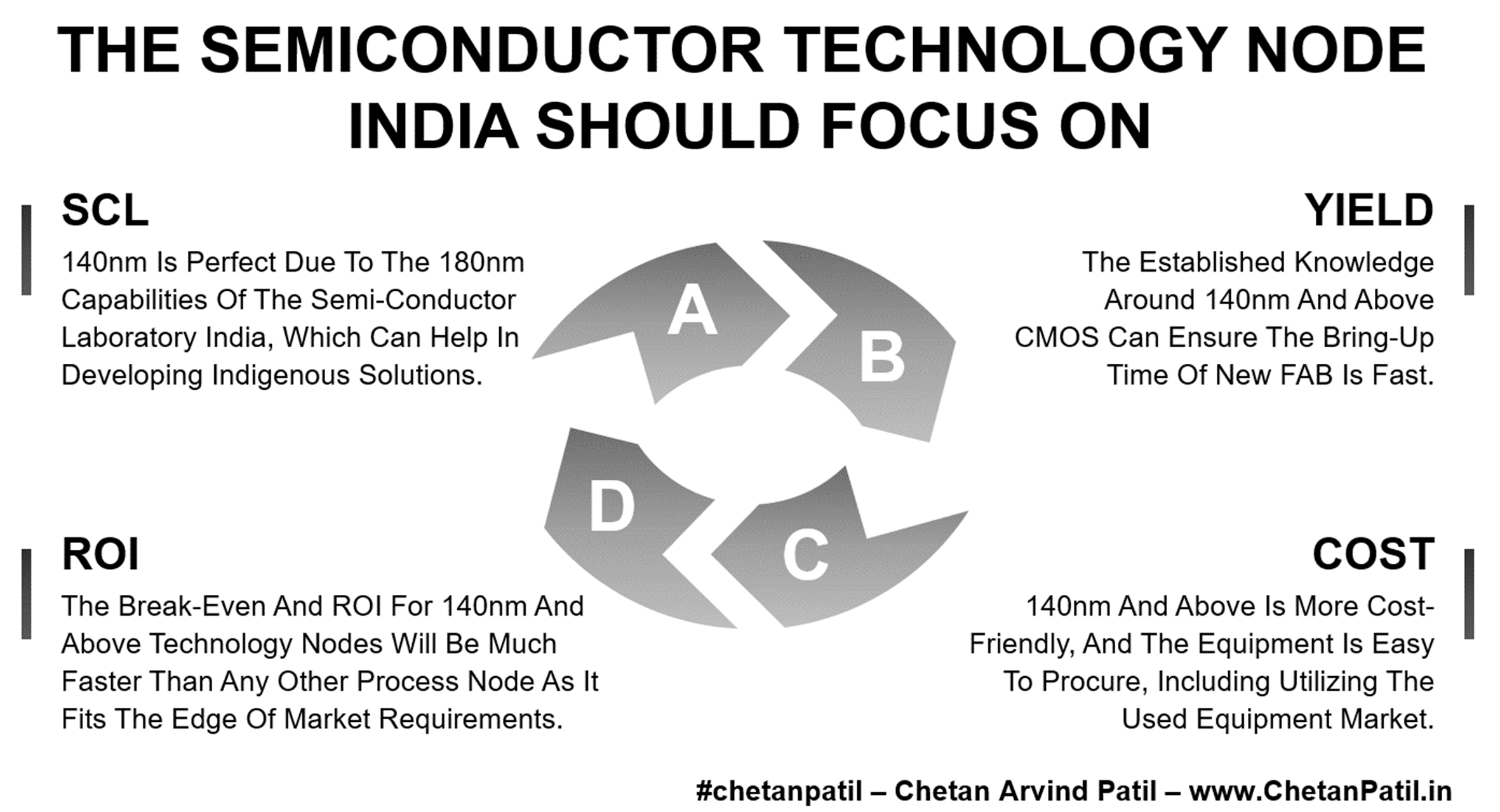
    Thus, considering the capabilities of India’s public semiconductor FAB, it is more suitable to aim for 140nm and above. The reason ranges from cost, yield, process control, and market demand. 140nm is also perfect due to the 180nm capabilities of the Semi-Conductor Laboratory, which can extend to not only develop CMOS devices to fabricate 140nm but can potentially ensure that these facilities also get upgraded – a win-win situation for all.

    If the SCL cannot develop 140nm in-house, there is also a potential to tie up with established Pure-Play vendors. Similar to Maruti-Suzuki JV. Regarding market potential, 140nm CMOS, including BiCMOS semiconductor technology, is still in high demand, mainly in the industrial, automotive, mobile, and other computing sectors.


    Picture By Chetan Arvind Patil

    The semiconductor equipment and setup cost for 140nm and above CMOS/BiCOMS semiconductor FAB is relatively lower than the advanced nodes. Yield is better, and the application area is far greater. Focusing on anything lower, mainly the advanced nodes like 7nm, etc., will be a step in the wrong direction unless a private player is willing to set up FAB by utilizing the incentives and spending endless resources.

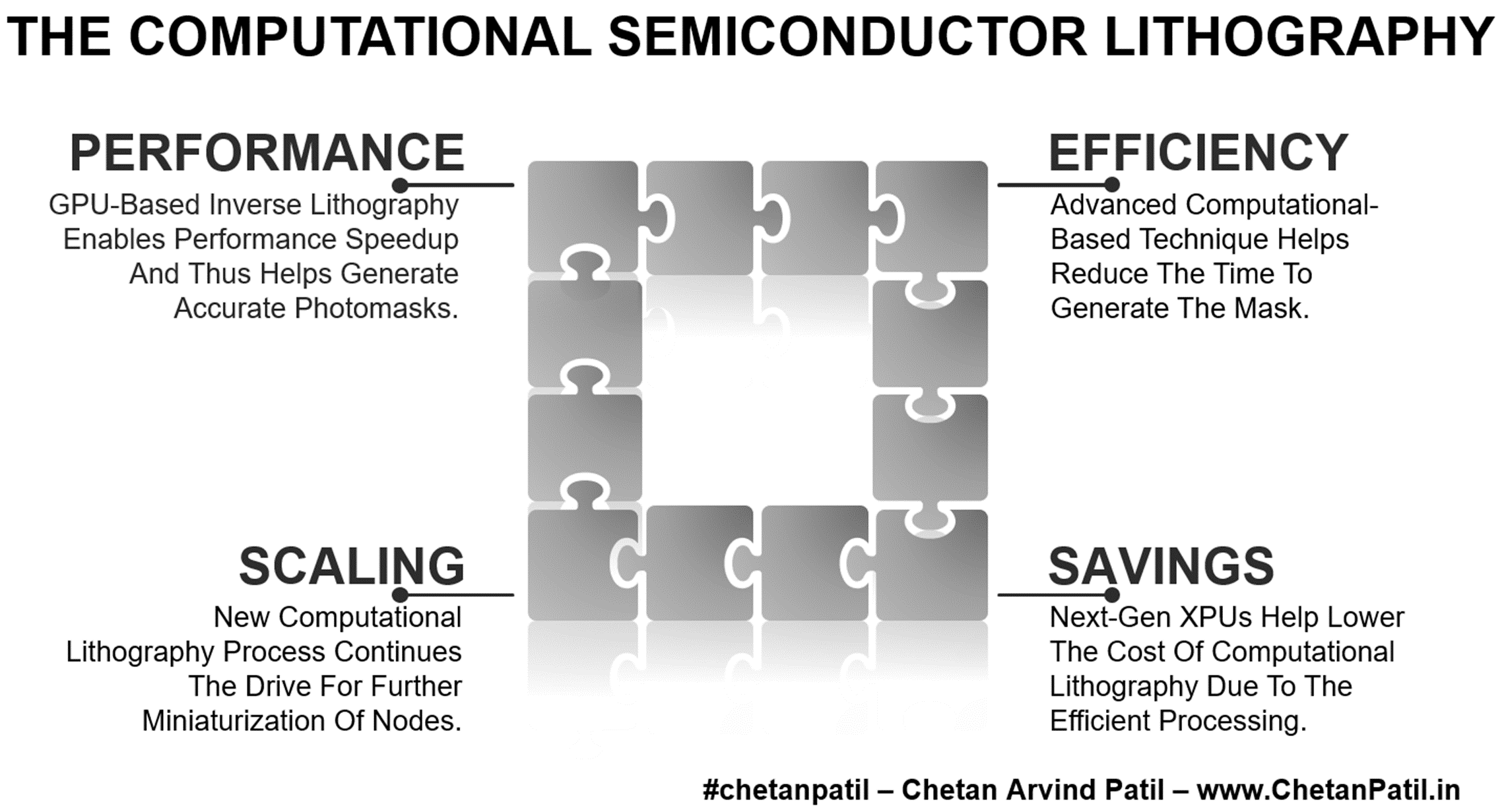
    Benefits of 140nm and above CMOS/BiCMOS:

    Proven: 140nm and above is an established and widely used technology node that can speed up India’s semiconductor fabrication and manufacturing entry.

    Cost: 140nm and above is more cost-friendly, and the equipment is easy to procure, including utilizing the used equipment market.

    Yield: The established knowledge around 140nm and above CMOS can ensure the bring-up time of new FAB is fast.

    ROI: The break-even and ROI for 140nm and above technology nodes will be much faster than any other process node as it fits the edge of market requirements.

    While having an advanced node FAB in India can be a game-changer, but only if a private player does it. If the focus is to get Indian companies to set up FAB in India (like Vedanta, etc.), creating a tech JV with SCL and other players to develop process flow for 140nm and above indigenously could be a more significant breakthrough.


  • The Two Ways In Which Semiconductor EDA Tools Are Evolving For AI World

    Photo by David Schultz on Unsplash


    Electronic Design Automation (EDA) is integral to semiconductor product development. Over the last four decades, the EDA industry has revolutionized how chips get designed, verified, simulated, and validated. During this time, EDA vendors have also adapted to different changing computing landscapes.

    For example, the early use cases of EDA solutions used to be more local and then, with the advent of servers, became more remote. Similarly, EDA vendors have adopted cloud solutions for better performance and reliability.

    Moving to the cloud has also enabled a more decentralized way of designing silicon chips. It provides a more secure form of developing an idea into a working software prototype. It has also streamlined how IPs are delivered, and licenses are maintained. In turn, the cloud also allows IP developers to ship the required files on the go swiftly.

    As the complexity of the silicon design increases with the increase in features, the runtime of simulation also increases, and by adopting the cloud for EDA, the vendors can now provide scalable, high-performance computing, which shortens design validation and closure time.


    Picture By Chetan Arvind Patil

    Now, the latest feature adoption for the EDA ecosystem is the AI. There are two different main ways in which EDA vendors have to accept and adopt the AI ecosystem for chip design and development:

    First Front: Enabling AI features in the EDA tool suite and ensuring the customers make the most of it. It is not directly related to design. More of a support system via AI.

    Second Front: Tackling standalone AI solutions that will be able to learn and design part of silicon chips and how it impacts EDA landscapes and business.

    Many of the top EDA vendors have already provided the solutions on the first front. However, the second front is a tricky and new arena.

    It is a space that can go in favor or against the EDA vendors. Why: If today, AI can assist in chip development, then tomorrow, what is stopping AI framework developers from creating an ecosystem?

    True, this is not as easy as it sounds, and on paper, it looks fantastic, but in reality, it may be more challenging. Nevertheless, shortly, someone may create an AI framework purely for the chip designing domain to capture and learn by generating the data independently. The tricky part will be to prove the solutions, but that is where experienced semiconductor engineers will always come into the picture.

    With Google, Microsoft, Amazon, and other cloud vendors moving into the semiconductor cloud EDA ecosystem, the probability of second front becoming a reality is very high, as these companies are already leading the AI front and adopting the solutions for AI self-designing chips is not going to be a tricky part.

    Eventually, both fronts are new opportunities for the semiconductor EAD landscape and might open more market opportunities for EDA vendors than ever. Only time will show how these two fronts will evolve, and a lot depends upon how fast or slow the semiconductor design companies embrace AI for silicon product development.


  • The Need Of Assistive Generative AI In Semiconductor Design And Manufacturing

    Photo by Brecht Corbeel on Unsplash


    Generative AI (GenAI) is creating new ideas and the market for the software industry. Software developers are using GenAI to develop tools to revolutionize the digital world. Per experts, we are only getting started with GenAI. And, at some point, the semiconductor industry will have to adapt to the GenAI way of working.

    Examples of how GenAI can help with semiconductor design and manufacturing:

    Design: Smarter EDA tool can speed up the process of design development. It can be done by GenAI taking over the repetitive tasks. GenAI can also capture errors on the go and suggest better design optimization techniques. And slowly, based on the historical data, help designers build optimized solutions.

    Simulation: Simulating the design and capturing the data to validate the specification is critical to the semiconductor design process. As the complexity of the circuit design increases, the GenAI-based simulation tools can help the designer by providing better-summarized data, swiftly comparing it with similar past design databases to reveal critical insights and, in turn, can also develop new models to predict different reliability to characterization profiles accurately.

    Defect Generation: Process control and yield management are critical to achieving the highest ROI in any semiconductor manufacturing environment. GenAI can help generate defects that can occur with ultra-advanced semiconductor nodes. This information can enable faster and more accurate classification of yield issues and capture issues on the go.

    Planning: As much as semiconductor design and manufacturing is about technical understanding, a lot also depends on the planning aspect. Aside from resources, scheduling, and development, it is vital to product launch. GenAI can be a game changer by creating better flows of executing and planning by considering different data points from past learnings and failures.

    While GenAI itself will not be able to take over 100% of the design and manufacturing process of semiconductor products, on the other hand, it can act as a catalyst to help drive assistive design and manufacturing.

    It is precisely the type of solution the semiconductor industry needs so that the advanced semiconductor technologies around Moore’s law and More Than Moore drive new design and manufacturing methods forward faster.


    Picture By Chetan Arvind Patil

    The impact of slowly deploying semiconductor-focused GenAI solutions will have a positive effect on the way the design and manufacturing of semiconductors occurs.

    The significant benefits of utilizing the GenAI capabilities are as follows:

    Time: Assist in the silicon block design and provide a better view of further optimizing for performance, power, and area. The assistance by GenAI, based on historical data, can improve the design and manufacturing process and help semiconductor engineers iterate faster than ever.

    Corrections: Finding bugs in the design and manufacturing flows and presenting them ahead of time is also something GenAI can help the semiconductor industry with. It can significantly reduce costs and drive companies towards defect-free products.

    Efficiency: One of the fundamental goals of any new silicon chip or process node is to improve performance and manage power/energy consumption. To build better efficient designs and processes, reviewing historical data is critical. And this is where GenAI can bring a gaming-changing solution and assist design/manufacturing teams in speeding up the process.

    Cost: If the solutions around GenAI can reduce the design/manufacturing time, bring zero defect products and reduce the silicon ideation to validation to sampling to production time, then the potential cost benefits are many.

    Confidentiality is one of the biggest hurdles in deploying GenAI solutions in the semiconductor industry. To some extent is a valid concern, as the semiconductor companies will never know how deploying GenAI solutions can lead to critical information leakage, which can be catastrophic.

    To tackle this, semiconductor design and manufacturing companies must develop a process allowing them to build GenAI-specific tools in-house or, at the least, trust the vendors they are working with to provide a tailored solution that ensures the sandbox created is complete and leakproof.

    Eventually, the semiconductor industry has to catch up with the software industry on the GenAI front. Otherwise, the development speed in the software domain will be 100x, and the semiconductor industry will follow the 10x speed, creating new age bottlenecks for both sectors.


  • The Semiconductor Coopetition Is On Rise

    Photo by Pascal Swier on Unsplash


    Coopetition is a business strategy that combines competition and cooperation. In the semiconductor industry, coopetition can take many forms, such as:

    Joint Ventures: Collaborate to develop a new product or technology.

    Alliance: Resources or expertise sharing to achieve a common goal.

    Open Source: Contribute to open-source software and hardware.

    Standards: Work together to develop industry standards that can speed up the adoption of new technologies.

    Coopetition can be a beneficial strategy for the semiconductor industry because it can help to:

    Cost: Sharing resources and expertise can create common grounds for managing increasing costs.

    Innovation: Companies can share ideas and knowledge by working together, leading to innovations.

    Market Access: By cooperating, companies can access new markets and customers.

    Competition: Coopetition strengthens the semiconductor industry and makes it more competitive.


    Picture By Chetan Arvind Patil

    Over the last few years, coopetition has increased around the semiconductor industry. It shows how semiconductor-dependent companies align their business to what works best for the market.

    Some of the examples of coopetition are from the semiconductor industry:

    TSMC, Bosch, Infineon, And NXP Jointly Invest In European Semiconductor Manufacturing Company (ESMC).

    Bosch, Infineon, Nordic, NXP, And Qualcomm Jointly Invest In A Company Aimed At Advancing The Adoption Of RISC-V Globally By Enabling Next-Generation Hardware Development.

    Mediatek Partners With NVIDIA To Provide Full-Scale Product Roadmap To The Automotive Industry.

    NVIDIA, ASML, TSMC, And Synopsys Set Foundation For Next-Generation Chip Manufacturing.

    Apple Announces Multibillion-Dollar Deal With Broadcom For Components Made In The USA.

    Qualcomm Announces Multi-Year Collaboration With Sony To Deliver Next Generation Smartphones.

    Qualcomm Collaborates With Hyundai Motor Group On Purpose-Built Vehicle Infotainment.

    Intel, Ericsson Expand Collaboration To Advance Next-Gen Optimized 5G Infrastructure.

    Synopsys And Samsung Foundry Deepen Collaboration To Accelerate Multi-Die System Design For Advanced Samsung Processes.

    Synopsys And Arm Strengthen Collaboration For Faster Bring-Up Of Next-Generation Mobile SoC Designs On The Most Advanced Nodes.

    Synopsys And Samsung Collaborate To Deliver Broad IP Portfolio Across All Advanced Samsung Foundry Processes.

    Cadence Extends Collaboration With TSMC And Microsoft To Advance Giga-Scale Physical Verification In The Cloud.

    Intel And ASML Strengthen Their Collaboration To Drive High-NA Into Manufacturing In 2025.

    Imec And ASML Sign Memorandum Of Understanding (MoU) To Support Semiconductor Research And Sustainable Innovation In Europe.

    AMD And Qualcomm Collaborate To Optimize Fast Connect Connectivity Solutions For AMD Ryzen Processors.

    And, The List Goes On….

    However, coopetition can also be challenging, requiring companies to balance their competitive and cooperative interests. It is essential for companies to carefully consider the risks and benefits of coopetition before entering into a coopetition arrangement.

    Nevertheless, as the semiconductor industry evolves around the AI and More Than Moore strategy, one can expect to see even more coopetition arrangements.


  • The Semiconductor For X

    Photo by Thufeil M on Unsplash


    Semiconductor Design for X (DFX) is a set of principles that can be applied to any product to improve its manufacturability, testability, reliability, and other critical technical aspects. With the ever-increasing complexity of semiconductor products, it has become crucial to ensure the DFX methodologies are applied correctly.

    The semiconductor DFX methodology helps by improving following:

    Manufacturability: DFX techniques make semiconductors easier to manufacture, which can lead to lower costs and higher yields. For example, the DFX techniques can reduce the number of process steps required to manufacture a semiconductor or make the process steps more robust to variations in materials and equipment.

    Testability: DFX makes it easier to test semiconductors, which can lead to higher-quality products. For example, DFX techniques create design test points in a semiconductor.

    Reliability: DFX drives semiconductors to be more reliable, which can lead to longer product lifetimes. For example, DFX techniques can ensure the design of semiconductors with better thermal or aging schemes.

    These are just a few examples of semiconductor design for X. There are many other considerations that semiconductor engineers must take into account when designing a semiconductor, such as materials, layout, and manufacturing flow.

    Materials: The choice of materials can significantly impact the manufacturability of a design. Semiconductor engineers must carefully consider the materials’ properties to ensure the semiconductor design can be manufactured cost-effectively.

    Design Layout: The design flow is also a critical DFM consideration. The process must ensure that the design can be manufactured efficiently. Semiconductor engineers use various tools and techniques to maximize the layout of a plan, such as floor planning, placement, and routing.

    Manufacturing Process: The manufacturing process itself can also significantly impact the manufacturability of a design. If not controlled, then it can lead to higher defects and ensure the plan meets the desired specifications. Semiconductor engineers must work closely with manufacturing engineers to ensure the design can get reliably manufactured.


    Picture By Chetan Arvind Patil

    In addition to the above, applying the DFX methods improves several critical aspects of semiconductor products:

    Performance: Improves the performance of semiconductors by reducing power consumption, increasing speed, or improving accuracy.

    Security: Increase the security of semiconductors by making them more resistant to tampering or hacking.

    Cost: Reduce the cost of semiconductors by making them easier to manufacture, test, and assemble.

    Variability: Helps in the reduction of variability of semiconductor process. It means that machines will be more consistent in their performance, which can improve reliability and quality.

    Variability: Helps in the reduction of variability of the semiconductor process. It means that machines will be more consistent in their performance, which can improve reliability and quality.

    Yield: DFX can also help improve the product yield by reviewing the process, devices, and other functional aspects thoroughly before fabrication.

    DFX has been a critical part of the semiconductor design process. By considering manufacturability, power, variability, cost, yield, and reliability from the earliest stages of design, semiconductor manufacturers can improve their products’ quality and performance while reducing costs and time to market.


  • The Semiconductor AI Will Design The Silicon It Needs

    Photo by Google DeepMind on Unsplash


    Artificial General Intelligence (AGI) is a hypothetical type of artificial intelligence that can understand or learn any intellectual task a human can. AGI is still a long way off, but if achieved, it could profoundly impact several technological areas, including the design of silicon chips used for AI applications.

    One of the biggest challenges in designing silicon chips is balancing performance with power consumption, apart from enabling a set of blocks to process and manage the workload without slowing down the system. As chips become more powerful, they also become more power-hungry. AGI could solve this problem by identifying the bottlenecks in current silicon chip designs across numerous fragments and their workloads. AGI could then use this information to develop unique design architectures that are more efficient and power-friendly.

    AGI: Artificial General Intelligence (AGI) Is Still A Long Way Off. If Achieved, It Could Profoundly Impact Several Technological Areas, Including The Design Of Silicon Chips.

    Chips: AGI Could Solve This Problem By Iterating Through Numerous Solutions To Come Up With The Best AI Suited Chips.

    In addition to improving performance and power efficiency, AGI could also help design silicon chips tailored explicitly for AI applications. For example, AGI could design chips better at processing large amounts of data or more efficient at learning new patterns. It will be able to do so due to capturing the ins and outs of how different workloads have performed. Currently, this task is very manual, and with AGI, it is possible to speed up the analysis flow tremendously.

    Another example: AGI might identify that the chip’s memory bandwidth is a bottleneck. It means the chip cannot access its memory fast enough (compared to the expectation) to meet the application’s demands. AGI would then use this information to develop a new design architecture that improves the chip’s memory bandwidth.


    Picture By Chetan Arvind Patil

    AGI will use data and modeling to design next-gen AI silicon chips in several ways. First, AGI will capture data from numerous existing chips to identify the commonality in lack of performance. This data will include information about the types of AI applications, the amount of data these applications need to process, and the available power budget.

    Second, AGI will use models to predict the performance of different chip architectures. These models will be per the AGI’s data from current chips. AGI will use these models to evaluate other design options and choose the one most likely to meet the performance requirements of future chips.

    Model: AGI Will Use Models To Evaluate Numerous Design Options And Can Pick The One Best Suited For Future Workloads.

    Future: AGI Could Also Revolutionize Neuromorphic Silicon Chip Development.

    Finally, AGI will combine data and models to optimize the design of next-gen AI silicon chips. This optimization will include factors such as the chip’s architecture, the size of its transistors, and the materials used to build it. AGI will also use its knowledge of physics and chemistry to optimize the chip’s design for performance, power efficiency, and scalability.

    The development of AGI for silicon chips is still in its early stages, with few examples of designing chips on its own. However, it has the potential to revolutionize the way that we design and build silicon chips. By working together, AGI and neuromorphic silicon chips could create a new generation that is more powerful, efficient, and scalable than possible.


  • The Semiconductor Is More Basic Science Than Applied

    Photo by Trnava University on Unsplash


    Semiconductor engineering is a field that distinguishes basic and applied science. On the one hand, it relies on a deep understanding of fundamental physics, such as the behavior of electrons in solids. On the other hand, it also requires the ability to apply this knowledge to the design and manufacture of practical devices.

    In recent years, semiconductor engineering has become increasingly reliant on basic science. It is because the challenges of miniaturizing and improving semiconductor devices are becoming increasingly complex. To address these challenges, semiconductor engineers must deeply understand the underlying physical principles.

    Examples of how chemistry, physics, and mathematics find use in semiconductor engineering:

    Chemistry: Chemists study the structure and properties of matter, including semiconductor materials. This knowledge drives the development of new semiconductor materials with improved properties, such as higher electron mobility or lower carrier concentration. For example, chemists have developed new methods for growing silicon crystals with fewer defects, which has led to the development of smaller and faster transistors.

    Physics: Physicists study the behavior of matter at the atomic and subatomic levels. This knowledge helps in understanding the behavior of electrons in semiconductor materials, which is essential for designing semiconductor devices. For example, physicists have developed models that describe how electrons move through semiconductor materials, which helps create transistors that operate at high frequencies.

    Mathematics: Mathematicians use their knowledge of numbers and logic to solve problems in various fields, including semiconductor engineering. For example, mathematicians use statistics to analyze the performance of semiconductor devices, and they use calculus to design semiconductor circuits.

    In addition to design, basic science plays an increasingly important role in semiconductor manufacturing. For example, developing new lithography techniques requires a deep understanding of the physics of light and matter.


    Picture By Chetan Arvind Patil

    The field of semiconductor engineering is rapidly evolving, and the demand for semiconductor engineers with a strong foundation in basic science will grow in the coming years. It is crucial to ensure the basic science behind the design and manufacturing of semiconductors progresses forward.

    Design: In design, basic science enables the development of new transistor materials and structures. For example, researchers are using carbon nanotubes and graphene to create smaller and faster transistors than traditional silicon transistors.

    Manufacturing: Basic science drives new lithography techniques in manufacturing that produce smaller and more precise features. For example, researchers use extreme ultraviolet (EUV) lithography to create parts that are just a few nanometers.

    As the challenges of miniaturizing and improving semiconductor devices become more complex, semiconductor engineers will need to understand the underlying physical principles deeply. It will require close collaboration between semiconductor engineers, physicists, chemists, and materials scientists, thus opening up opportunities for science undergraduate and graduate students.


  • The Semiconductor AI Dependency

    The Semiconductor AI Dependency

    Photo by Bill Fairs on Unsplash


    Artificial Intelligence (AI) is a rapidly growing field revolutionizing many industries. However, AI highly depends on semiconductors, the electronic components that power computers and other devices.

    Semiconductors are essential for AI because they provide the processing power and memory needed to run AI algorithms. For example, AI algorithms for image recognition require a lot of processing power to analyze large images. AI algorithms for natural language processing require a lot of memory to store and process large amounts of text data.

    Essential: Semiconductors Are Essential For AI In Providing The Required Processing Power.

    Demand: Semiconductors For AI Will Grow Exponentially In The Coming Years.

    The demand for semiconductors for AI will grow exponentially in the coming years. It is because AI is getting deployed in more and more applications, such as self-driving cars, healthcare, and manufacturing.

    The growth of AI also drives innovation in semiconductor design and manufacturing. For example, advanced semiconductor materials provide the performance and power efficiency needed for AI applications.


    Picture By Chetan Arvind Patil

    Semiconductor design is also critical to AI chips’ performance and efficiency. As AI algorithms become more complex, semiconductor designers will need to develop new ways to optimize the performance of AI chips. For example, semiconductor designers will need to find ways to reduce the power consumption of AI silicon while still maintaining high performance.

    Semiconductor manufacturing is also a critical factor in the performance and cost of AI chips. As the demand for AI chips grows, semiconductor manufacturers will need to find ways to increase the production capacity of AI chips. In addition, semiconductor manufacturers will need to find ways to reduce the cost of AI chips while still maintaining high quality.

    Manufacturing: Semiconductor Equipment And Materials Are Also Essential Factors In The Production Of AI Chips.

    Dependent: The Future Of AI Is Highly Dependent On The Semiconductor Industry’s Roadmap.

    Semiconductor equipment and materials are also essential factors in the production of AI chips. As the demand for AI chips grows, semiconductor equipment and materials suppliers will need to develop new technologies that can meet the needs of AI chip manufacturers.

    The future of AI is highly dependent on the semiconductor industry’s roadmap. As AI continues to grow, the demand for semiconductors will also increase. It will drive semiconductor design, manufacturing, equipment, and materials innovation. Developing new semiconductor technologies will help make AI more powerful, efficient, and affordable – an existing time for both the AI and semiconductor industry.


  • The Semiconductor FATE Is FAST

    Photo by Raphael GB on Unsplash


    The semiconductor manufacturing business model is changing from FATE to FAST. FATE stands for Fabrication, Assembly, and TEesting, while FAST covers full-flow, i.e., Fabrication, ASsembly, and Testing.

    In the FATE model, the fabrication of semiconductor chips is with one specific company, while a different semiconductor manufacturer provides assembly and testing services. In the FAST model, a single semiconductor manufacturer performs all three steps of the manufacturing process.

    FATE: Fabrication, Assembly, And TEsting. The Fabrication Of Semiconductor Chips Is With One Specific Company, While A Different Semiconductor Manufacturer Provides Assembly And Testing Services.

    There are several reasons why the semiconductor manufacturing business model is changing from FATE to FAST. One reason is that it can help to reduce costs by performing all three steps of the manufacturing process under one roof and, in a few cases, also performing in-house. It can also bring significant cost savings due to turnkey flow, especially for high-volume customers.

    Another reason for the shift to FAST is that it can help to improve quality. When a single company performs all three critical steps of the semiconductor manufacturing process, it has more control over the quality of the final product. It can lead to fewer defects and a higher yield.


    Picture By Chetan Arvind Patil

    The shift to FAST can also benefit customers. By having a single point of contact for all three steps of the manufacturing process, customers can streamline their supply chains and reduce the time it takes to get their products to market. It can give them a competitive advantage in the marketplace.

    Of course, there are also some potential downsides to the FAST model. One concern is that it could decrease innovation and, in many cases, will add extra cost to the manufacturer as the upfront investment to set up such a turnkey facility is very high. If fewer companies are involved in manufacturing, there may be less incentive to develop new and improved technologies, mainly for the aging process, that are still widely used for diverse applications.

    FAST: Fabrication, ASsembly, And Testing. Covers Full-Flow. A Single Semiconductor Manufacturer Performs All Three Steps Of The Manufacturing Process.

    Another concern is that the FAST model could lead to increased market concentration. If a few large companies control the entire semiconductor manufacturing process, it could be more difficult for new companies to enter the market.

    The shift from FATE to FAST can significantly change the semiconductor manufacturing industry. It has the potential to benefit both customers and manufacturers, but there are also some potential downsides to consider. Only time will tell how the FAST model will ultimately impact the industry.


  • The Computational Semiconductor Lithography

    Photo by Dan Cristian Pădureț on Unsplash


    Computational lithography is a specialized field in the semiconductor manufacturing domain. It is used during lithography when advanced algorithmic models optimize the patterning and masking process. It is done by deforming the patterns to compensate for the physical and chemical effects naturally occurring in a standard flow. It utilizes the concept of inverse lithography to do so.

    Result: Accurate production of the desired chip patterns on the wafer to fabricate the complex advanced node silicon.

    Achieving such a complex and exact process on the go demands compute speed. It means that the equipment must either be equipped with high-performance XPUs to deliver a modeling approach or be able to offload and on load. In practice, the remote and distributed processing approach is better suited.

    Performance: GPU-based inverse lithography enables performance speedup and thus helps generate accurate photomasks.

    Efficiency: Advanced computational-based technique helps reduce the time to generate the mask.

    However, as the complexity of the technology node increases, it has become challenging to keep up with the processing requirements of lithography. Thus, better XPUs and also software support is required.


    Picture By Chetan Arvind Patil

    To tackle this bottleneck, NVIDIA, Synopsis, TSMC, and ASML have collaborated to leverage the software libraries on the GPU architectures. It will help drive silicon scaling and enable their end users to reduce costs and accelerate technology advancements. It leverages GPU-based inverse lithography.

    Below is a simplified flow of what this collaboration will speed up further. Details around the litho library (cuLitho) were presented by Vivek K Singh, Vice President, Advanced Technology Group, NVIDIA, early this year.


    Image Source: NVIDIA
    Image Source: NVIDIA
    Image Source: NVIDIA
    Image Source: NVIDIA

    It is a significant step in the right direction when there is a proper set of collaborators: Covering GPU, EDA, Technology-Node, and Semiconductor Equipment experts.

    Today, the compute workloads that achieve computational lithography are the most complex and extensive computational activity ever executed during semiconductor production.

    Savings: Using next-gen XPUs help lower the cost of computational lithography due to the efficient processing.

    Scaling: New computational lithography process continues the drive for further miniaturization of nodes.

    With the latest advancements in GPU technology and the collaborative approach, computational lithography performance will skyrocket.

    Eventually, semiconductor manufacturers will now achieve unprecedented speed and accuracy for all the lithography requirements. Such an improvement will also help drive better die-level manufacturing accuracy, improved yield, and the ability to continue to scale into the Angstrom era.