Blog

  • The Semiconductor Data And Future Implications

    Photo by Mathew Schwartz on Unsplash


    Data has become more relevant than ever for semiconductor product development. More so when the applications of silicon devices are increasing year after year and touching every aspect of day-to-day life. As the semiconductor data complexity increase

    This increase in the importance of semiconductor data has pushed companies to invest in the resources required to drive data collection at every step of product development. The primary focus is to capture and analyze data to deliver high-quality products.

    Application: Application Types Are Increasing The Complexity Of Semiconductor Data.

    Analysis: The Cost Of Semiconductor Data Analysis Is Increasing With The Increasing Complexity.

    The increase in application and use cases of silicon devices also demands new equipment and tools that deliver the correct data. Even though several such solutions are already available, there is always a need to adapt these tools for the next-gen processes that require better accuracy and resolution, thus leading to new investment.

    The growing importance of data is the primary reason why the semiconductor industry has always found ways to capture data cleanly. Capturing relevant data has helped semiconductor design and manufacturing. However, as the reliance on semiconductor data grows, it is crucial to implement end-to-end data integrity.


    Picture By Chetan Arvind Patil

    The proliferation of semiconductor solutions in every aspect of life raises the question of whether the semiconductor data is the next-gen oil. Irrespective of it, the impact of semiconductor data and using it in the decision-making process has increased more than ever.

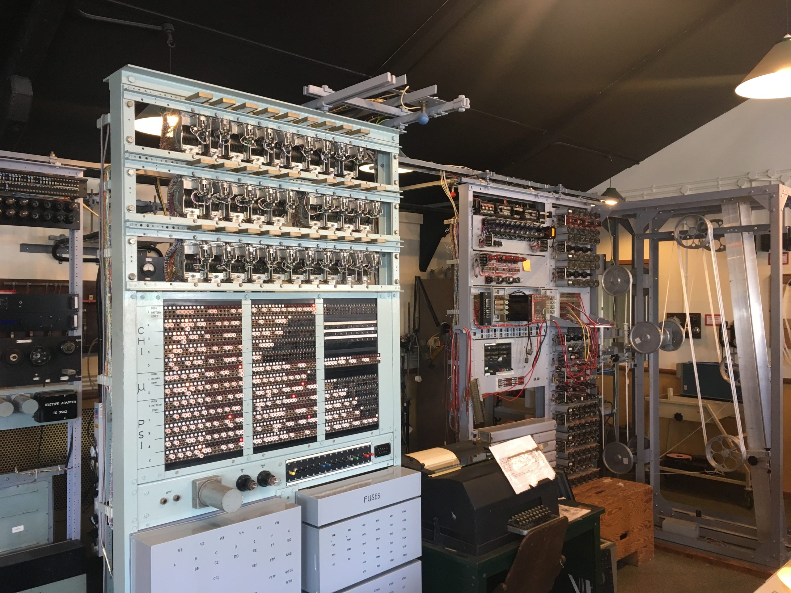
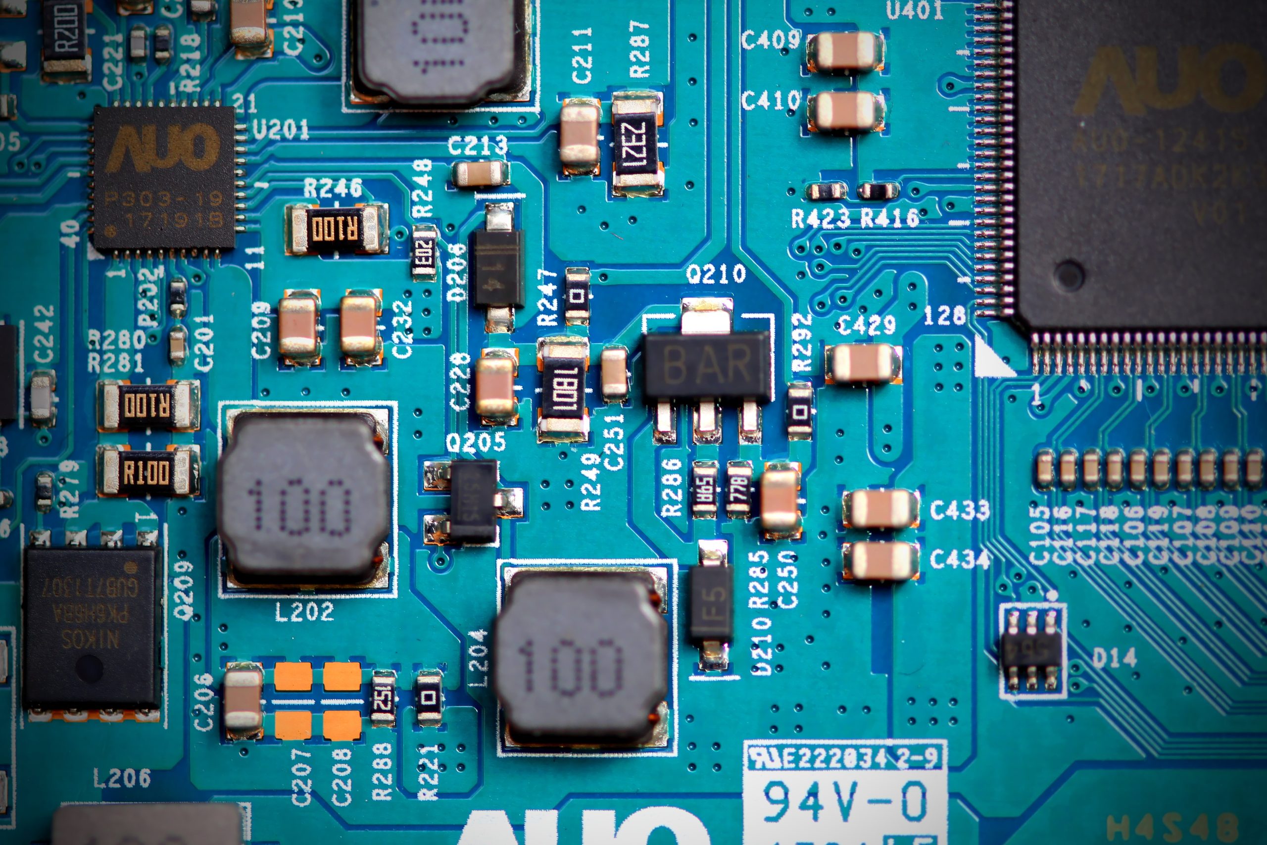
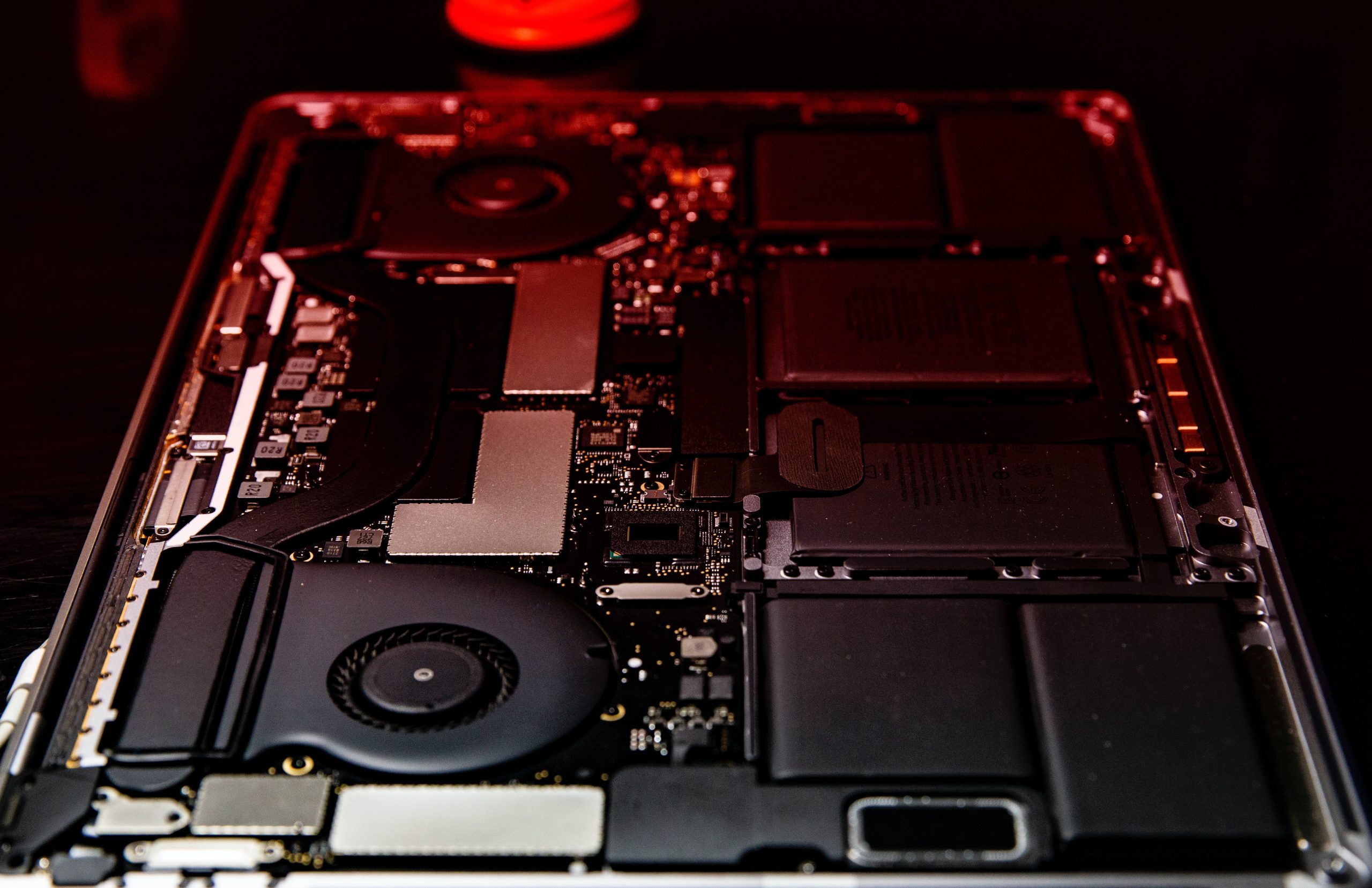
    Semiconductor manufacturing needs to be accurate, and any deviation can impact the production line. Semiconductor data during the fabrication and post-fabrication stages can reveal whether the product functions accurately. It can also provide insights to correct the issues before the product is shipped out.

    Impact: The Time To Analyze Semiconductor Data Is Increasing Due To Complex Processes.

    Quality: Semiconductor Data Helps Designers And Manufacturers To Provide High-Quality Products.

    Semiconductor data will become more critical during the angstrom era. Hence, it will be crucial for the semiconductor equipment industry to innovate solutions that ensure that complex and advanced products do not lead to data escapes. All this while also balancing the time and cost of semiconductor data.

    The journey of semiconductor data is an interesting one. It comes from different process steps that depend on several facilities, equipment, and human resources. And, to achieve high-quality silicon solutions, the need to deploy better and advanced data capturing and analysis will always increase.


  • The Semiconductor Market And Impact

    Photo by Patrick Perkins on Unsplash


    The semiconductor market has always followed the seesaw mode. With a seesaw, there are time intervals when the market has high demand followed by low demand. This trend impacts the semiconductor in different possible ways, and one of them is the long-term product development strategy.

    There is no easy way to control such a trend. The semiconductor industry should be pre-prepared and adapt based on the market feedback. It requires a mitigation plan, which should not impact product development and manufacturing.

    Market: Semiconductor Market Is Always In Seesaw Mode.

    Impact: Market Seesaw Impacts Long-Term Projections.

    The semiconductor market seesaw raises questions about whether a focused market approach is good or bad. Mainly for those semiconductor companies that are only catering to a specific market.

    One better way to manage the impact of the market is to diversify the products. Such a strategy enables companies to be more resilient, which benefits the industry during the phases when the market demand is not as expected.


    Picture By Chetan Arvind Patil

    In the coming years, the semiconductor industry will need to develop trillion more silicon devices. It requires robust planning that balances the design and manufacturing capacity.

    For such targets, the market seesaw movement also plays a crucial role. Thus, raising the need to capture the upward/downward trend before it occurs, as it can allow more proactive planning than reactive.

    Future: More Robust Future Planning Is Required.

    Trend: Seesaw Trend Is Expected To Continue Forever.

    The trend and the future of the semiconductor market will always keep changing. Thus, making it difficult to capture the ripple effect. It presents a unique challenge and opportunity for companies to develop predictive tools that can capture the future trend and then alert in advance on how to manage operational activities.

    Market impact on the semiconductor or any other industry will be a deciding factor in driving the future course of action. What is crucial is to capture the such trend and then divert resources to mitigate any ripple effect. More so when the impact is on a high-tech industry like a semiconductor.


  • The Always Increasing Semiconductor Speed

    Photo by Farai Gandiya on Unsplash


    Semiconductor speed is dependent on performance characteristics. These characteristics define the operating states and how fast or slow the silicon-based system will operate.

    Over the last five decades, the semiconductor speed has only increased exponentially. Consider the example of the CPU core. Today, the latest generation CPU has a clock speed of 4.3 GHz, which executes 4.3 billion cycles per second. Such performance is a crucial factor in the development of widely deployed advanced and complex applications.

    Speed: Silicon Speed Is Vital In Driving Different Types Of Use Cases.

    Impact: Operating Features Are Key In Enabling New Types Of Semiconductor Products.

    Semiconductor speed is dependent on several factors. The chip architects have to consider different technical scenarios and create a design scheme that will not only cater to the consumer’s request but also pushes the development of new features that can help the industry move forward.

    However, it is not always possible to manage the semiconductor speed. There are technical (datapath, NoC, memory, computation bottleneck, cache memory, latency, etc.) reasons that make the process of increasing the semiconductor speed a slow one.


    Picture By Chetan Arvind Patil

    Overcoming speed-based bottlenecks requires novel silicon design and manufacturing approaches. It is also the main reason the semiconductor industry to focuses on new processes that can take the area-driven speed out of the equation.

    Chiplets, heterogenous, fusion design, and die-stacking are a few novel approaches being adopted. In all cases, the primary goal is to remove the area-based feature from the equation.

    Application: Application Usage Is Greatly Affected By The Silicon Speed.

    Cost: Using A Specific Speed-Based Silicon Solutions Impacts Product Cost.

    As the semiconductor industry moves towards more advanced technology nodes, the focus on semiconductor speed will increase. The fundamental reason is the challenges due to the smaller FET area leading to a smaller die area. It provides small room to increase the clock level speed.

    Today, the industry is closer to touching 5GHz of clock speed for XPU devices. There is little to no room for further speed improvement using the traditional approach. It creates new challenges that the semiconductor industry will for sure overcome.


  • The Balancing Act Of Semiconductor FAB And OSAT

    Photo by Christophe Hautier on Unsplash


    Semiconductor manufacturing relies heavily on the semiconductor FAB and OSAT. Semiconductor FAB turns the design into fabricated wafers. On another side, OSATs convert fabricated wafers into finished goods. End customers to develop consumer and enterprise solutions using the finished goods.

    Semiconductor FAB and OSAT are so critical that any bottleneck can directly impact the semiconductor supply chain. It was already evident from the semiconductor shortage, which did impact all the industries that rely on it.

    FAB: The Capacity Of Semiconductor FABs Is Slowly But Surely Increasing To Meet The Demand.

    OSAT: Managing Capacity To Drive Back End Process Of Semiconductor Is Crucial.

    Such significant dependency and impact are the primary reason FABs and OSATs need a balanced capacity that provides options to different customers and ensures the semiconductor industry is positively growing.

    FABs and OSATs are also two different types of businesses. Managing these two requires a detailed overview of semiconductor technology node progress, assembly innovation, and testing developments. With the help of a technology roadmap, semiconductor manufacturing can also plan how to manage and expand capacity. As both FABs and OSATs need not grow in number together.


    Picture By Chetan Arvind Patil

    Worldwide, there is also a race to set up a semiconductor manufacturing ecosystem, and manufacturers have to take a call on whether to focus on FABs or OSATs.

    In this process, new semiconductor manufacturing ecosystems get attracted toward the FABs. The primary reason seems to be the innovation and significance of the semiconductor industry. However, the business side also plays a vital role in developing the new semiconductor manufacturing ecosystem. In the long term, it might be better to focus on OSATs and build an ecosystem of raw materials, testing equipment, and the talent trained at handling the assembly process.

    Balance: The Capacity Of FABs And OSATs Needs To Be Balanced So That Industry Has Options.

    Future: Future Of FABs And OSATs Relies Heavily On New Semiconductor Manufacturing Ecosystem.

    Then, using the platform created by the OSAT business, the new semiconductor manufacturing ecosystem can focus on building the FABs and thus slowly creating the end-to-end semiconductor manufacturing ecosystem. There are a few countries that have followed this process and have created a niche of their own.

    As the focus on building better and larger semiconductor FABs and OSATs grows, the crucial point will be which capacity to focus on and plan. So that it not only benefits the location but also pushes the semiconductor industry forward.


  • The Time Critical Semiconductor Supply

    Photo by CHUTTERSNAP on Unsplash


    The semiconductor supply chain ensures that the fabricated, assembled, and the tested product reaches customers on time. Achieving this goal requires eliminating all the bottlenecks that might impact the supply process.

    The standard process to mitigate bottlenecks is to capture the end-to-end supply chain requirements and then proactively fill the gaps. However, the better approach is to capture the supply time and ensure there are no time gaps.

    Inventory Time: How Long The Existing Supply Will Last.

    Reload Time: How Long Before The Supply Can Be Restored.

    In semiconductor supply, there are two ways to look at time: Inventory Time and Reload Time. The former provides a view of how long the inventory will last and later provides details about how much time it will take to replenish the stock.

    Eventually, the goal is to ensure there is never a shortage in the supply process. Nevertheless, it is not always the case, and the supply process is not bound to be smooth. More so when the semiconductor manufacturing process is cost and time sensitive, and there is no easy way to speed up the process.


    Picture By Chetan Arvind Patil

    Managing the Inventory Time and Reload Time has a positive impact on the semiconductor supply process. First of all, it eliminates hurdles and ensures the timely delivery of products. Second, it brings equilibrium in the demand and supply process, thus guaranteeing that customers never run out of the parts.

    As the semiconductor industry grows and the number of active products reach the trillion mark, the timely execution of an error-free supply process will play a huge part. It will require human resources to collaborate extensively to meet all the customer requirements on time.

    Impact: Proactively Eliminate Supply Chain Bottlenecks.

    Equilibrium: Ensuring The Right Amount Of Inventory, All The Time.

    The supply data management tools will also have to evolve and provide a better sneak by driving predictability. Thus, making the supply system more adaptive than reactive.

    In the end, the goal of the semiconductor supply chain is to meet the market demand. As the customer base expands, the challenge will be to ensure the market always has the right product delivered at the right time.


  • The New Semiconductor FAB Impact

    The New Semiconductor FAB Impact

    Photo by Anne Nygård on Unsplash


    In the coming few years, several new semiconductor FABs will start production. Several of these were part of long-term semiconductor requirements. Few started construction based on the semiconductor shortages and the push to mitigate such a scenario in the future. These new FAB required years of planning and have invested billions of dollars. Thus, the impact of these semiconductor FABs on the semiconductor industry is going to be significant.

    One of the impacts is the generation of employment, which will bring a new workforce to the semiconductor industry. It will also benefit the economy in the long term. And, for FABs situated closer to universities, such development can also drive industry-academia collaboration, which has the potential to keep supplying skilled resources.

    Employment: New Employment Generation Opens New Career Opportunity.

    Options: There Are Several Options For The Semiconductor Companies To Select From.

    Apart from employment, the new semiconductor FABs will provide more options to the semiconductor industry. These options will ensure the FAB-LESS companies have more FABs to reach out to and thus can also enables a way to diversify the manufacturing of their products.

    New semiconductor fabrication capacity also restores the supply and demand balance. Thus, reducing the overall cycle time. However, doing so demands time and continuous investment, and it is not always an easy process.


    Picture By Chetan Arvind Patil

    The positive impact of new semiconductor FABs is many and not limited to employment and options. However, there are also downsides to having more semiconductor FABs.

    One such downside is the oversupply or overcapacity. While new FABs are certainly going to provide more options to the industry. However, market demand also plays a key role. If the market demand is strong, the new FABs will be 100% occupied. If not, then there is a strong possibility that the new FABs might not be able to run at 100% throughput to drive the envisioned break-even point.

    Supply: Over Capacity Can Negatively Impact The Semiconductor Manufacturing Ecosystem.

    ROI: Market Demand Can Impact The Return On Investment.

    Negative market demand while the new FABs are coming up is not the best scenario. It raises questions about the ROI and also puts the investment at risk. While the FABs have already done the groundwork to mitigate such a situation. In many cases, it is not possible to eliminate such risks.

    The benefits of the new semiconductor FAB are positive only as it not only drives more capacity but also brings a new type of semiconductor technology that can benefit the semiconductor industry for the decades to come.


  • The Focus On Semiconductor Hyperscale

    The Focus On Semiconductor Hyperscale

    Photo by Thomas Jensen on Unsplash


    Data centers are vital for modern-day computing and have also evolved based on the requirements of different types of computing. Today, there are different types of data centers. However, of all, hyperscale data centers are on the rise.

    Hyperscale data centers house several connected computing systems. A typical hyperscale data center has around five thousand servers. Each of these has many high-end XPUs. As the number of hyperscale data centers increases, it will be crucial to equip these with more workload-friendly XPUs.

    Data: The Data Generation Rate Is Doubling Every Year Due To The Increase In The Number Of Connected Devices.

    Complexity: Complex Workloads Are Pushing The Need For New And Advanced Hyperscale Devices.

    Traditionally, the server version of the general-purpose architecture is enhanced and used for data centers. However, lately, companies that own hyperscale data centers have realized that the traditional approach is not future workloads friendly.

    To solve such a problem, in-house development of hyperscale XPUs is increasing rapidly. Such an approach enables the hyperscale data center to become more workload friendly. The primary reason is the workload requirements. These are better known to companies deploying hyperscale data centers. And, for such a use case, a custom in-house architecture for hyperscale XPUs can make the processing at such large data centers more energy friendly.


    Picture By Chetan Arvind Patil

    Not many companies have made in-house XPUs for hyperscale data centers. Only a select few have brought their research idea forward and have deployed solutions across different data centers. Others are still catching up and are focusing on specific CPU architecture to bring new types of data-centric XPUs. These new XPUs can be deployed in hyperscale centers to make them more workload and energy friendly than ever.

    It is also in the interest of hyperscale owners to invest in solutions that make their systems more cost-friendly. Eventually, the capital expenditure of the hyperscale data center is XPU servers. Any of the technical features (mainly thermal characteristics) that can be made more efficient than the predecessor, then in the long-term, it will lower the hyperscale ownership cost.

    Time: User Experience Is Now Heavily Driven By The Processing Time, And Hyper Scaling Is Critical To Achieve It.

    Scale: To Cater To Increasing Data Request, Data Centers Are Going In-House To Make Better Hyperscale XPU.

    Companies developing in-house custom hyperscale XPU need to plan carefully. Otherwise, they can end up spending more on hyperscale XPUs than focusing on services. In many cases, it is also better to collaborate and let dedicated XPU companies bring new solutions and adopt new products.

    As the number of hyperscale data centers increases, the requirement for better hyperscale-focused XPUs will increase. Those who can develop custom hyperscale XPU solutions that outperform existing solutions will disrupt the hyperscale market.


  • The Semiconductor Requirements For AI Chip

    The Semiconductor Requirements For AI Chip

    Photo by Markus Spiske on Unsplash


    The design and development of an AI Chip is not an easy process. More so when the cost is high while the use cases are limited. It thus makes the process of selecting requirements for an AI Chip a critical one.

    These requirements for AI Chip should be a balance of both software and hardware. On the software side, it is more about ensuring the correct set of tools and libraries are available to make the most of the underlying hardware architecture. From the hardware aspect, it is specifically about ensuring the semiconductor-driven processes used eventually can create the correct hardware for the specific application.

    Application: Application Requirements Should Drive The Design And Development Of AI Chip.

    Parallel: Parallel Computing Is The Core To Process AI-Inspired Workloads On The AI Chip.

    Application requirement is one of the core requirements of AI Chip. The primary reason is the cost. The application using the chip with AI-specific features should be able to make the case of ROI. Otherwise, the cost to develop, procure and use AI Chip will outweigh the gains.

    From the core technology point of view, AI Chip has to have the capability to drive parallel processing. Parallel computing has been around for decades and is de facto for any XPU. However, the premise falls short for AI applications due to the amount of data processing required while not adding latency. The data also keeps changing with the growing use case of AI.


    Picture By Chetan Arvind Patil

    Application and parallel computing certainly provide a way for AI Chip architects to select the right semiconductor design and manufacturing solutions. The chip architects of the AI Chip have to consider the precision and domain-specific requirements.

    For AI Chips, precision is about balancing speed and efficiency. The definition of speed and efficiency has changed as the application area has grown. However, the core concept is to ensure the user experience is not compromised. Otherwise, the AI system developed will be bottleneck driven.

    Precision: Balancing Speed And Efficiency Is Key To Driving Next-Gen AI Systems.

    Domain-Specific: System Level Software Architecture Should Align With The Requirements Of The AI Chip.

    Another aspect from a technical point of view is the domain-specific functionality. Utilizing parallel and precision computing also requires system-level software. It means it should be a domain-specific solution that allows software architecture to make the most of the silicon-level architectures.

    The race to develop different standalone and hybrid AI Chips will keep growing. Eventually, companies that balance cost and requirements will drive profitable AI Chip businesses.


  • The Semiconductor AI-XPU Adoption Race

    Photo by Markus Spiske on Unsplash


    Lately, several AI-driven silicon chip solutions have showcased the benefits of utilizing the semiconductor chips designed and manufactured for the AI application. It is also evident based on the several new XPUs being AI-compatible, which is possible only by combining the best features of CPUs, GPUs, FPGAs, and ASICs.

    AI-XPU: Silicon Chips Are Designed By Incorporating The Best Computing (CPU And FPGA) And Memory (GPU And ASIC) Technologies And Are Specialized For AI.

    Incorporating the best of CPUs, GPUs, FPGAs, and ASICs has thus given rise to AI-XPUs, which have features that can accelerate the processing of AI algorithms by incorporating the right set of compute-to-memory level features. Several processor-focused companies have already shown the benefits of such design and have created an adoption race for AI-XPU.

    AI Chip: Market For Chips That Are Adaptive And Can Efficiently Process Data Is On The Rise.

    Demand: AI-Driven Products Are Increasingly Demanding Better And Smarter Chip Solutions.

    Both the enterprise and consumer are utilizing AI-powered silicon. However, the use cases have been limited and have to evolve. Otherwise, the lower adoption rate will not enable new features for the AI-XPU.


    Picture By Chetan Arvind Patil

    The cost and time to design and manufacture AI-XPU are higher than the traditional general-purpose computing chips. The reason is the adoption rate. Unless AI-XPUs are mass-produced, they will be niche and capital-intensive. The market is demanding AI-powered silicon. However, it will be crucial to ensure the use cases of such applications are vetted. Otherwise, the cost and time spent will not provide the expected dividends.

    AI-XPU: AI-XPU Has Thus Become An Important Part Of The Race To Adopt Better Adaptive Solutions.

    Use Cases: Customers Will Have To Ensure The AI-XPUs Are Used For The Right Use Cases, Or Else Cost Will Rise.

    AI-XPU chips also face similar technical (memory, scaling, interconnect, etc.) hurdles as the traditional XPU chips. On the positive side, the advent of advanced packaging solutions and the growing use case of chiplets could be positive news for AI-XPU. Such new semiconductor design and manufacturing solutions can speed up the adoption of AI-XPUs.

    Computing demand will never go down. On the server side, the requirement to process data without adding latency will always grow. Thus, AI-XPU is a perfect fit for such use cases. Hence, faster adoption is crucial to make AI-XPU affordable.


  • The Semiconductor Enabling Technology

    Photo by John Jemison on Unsplash


    Developing new consumer and enterprise technology requires a new type of semiconductor technology, ranging from design, raw materials, equipment, packaging, fabrication, manufacturing, and many more segments of semiconductors.

    These technologies developed are called semiconductor enabling technology. Enabling technology brings a new type of semiconductor solution. These solutions push new products with features that are more efficient than ever.

    Few examples of enabling technology:

    xFETs

    Silicon Interposers

    Next-Gen xUV Equipment

    Advanced Automated Tools

    High-Speed Memory Interfaces

    New Semiconductor Packaging Solution

    And The List Goes On.

    Semiconductor enabling technologies are not easier to develop and do require thorough research and development. Even then, the probability of bringing a new enabling technology is low. Thus, as the first step, semiconductor companies should find the pressing issues in the existing solutions and then chart out a detailed plan to ensure the solution is error-free and has gone through a thorough validation plan.

    Research: Semiconductor Research And Development Is Key To Enabling New Technologies.

    Development: New Semiconductor Technology Demands Long-Term Investment.

    As with several high-tech industries, the cost to research and develop a semiconductor product is very high. Therefore, it makes the process of developing new solutions crucial and fragile. It also means investing in resources for the long term along with a backup plan in case of failure.


    Picture By Chetan Arvind Patil

    Knowledge building is key to finding if there is a fit for the new semiconductor-enabling technology. It focuses on ensuring the processes or new solutions developed will not only provide new features but will also fit in the semiconductor roadmap to bring the much-needed benefits.

    Building knowledge is about capturing the correct information by empowering the right resources. And doing so requires experienced talents who can figure out the possibilities of new semiconductor enabling technology and how it will best fit the requirements of future products.

    Knowledge: Building Knowledge Of New Semiconductor Solutions Requires Time And Resources.

    Implementation: Knowledge Coupled With Market Fit Is Must Before Implementing The Enabling Solutions.

    An example is an interposer. It not only found the perfect fit, but the solution pushed the semiconductor packaging industry towards a new era.

    As the semiconductor industry moves forward, more semiconductor solutions will reach different types of technical and business walls, and to overcome them, more futuristic semiconductor-enabling technologies will play a key role, and now is the right time to develop such solutions.