Blog

  • The Semiconductor Journey Ahead

    The Semiconductor Journey Ahead

    Photo by Emma Francis on Unsplash


    The semiconductor industry is going through one of the most exciting phases. Worldwide the demand for semiconductor-powered products is increasing and driving very high silicon demand that the semiconductor industry has never seen before. It has also re-ignited the debate to build more semiconductor design and manufacturing capacity, which in the long run is going to empower the semiconductor businesses and will increase the market reach.

    The spike in semiconductor demand also means that the industry will touch the trillion-dollar market. The path the semiconductor industry took to reach half of it has taken several decades, and in a very short time, it is set to grow by 50%. It showcases how the last few years have fueled the demand, and there is no denying that it will stay like this for years to come.

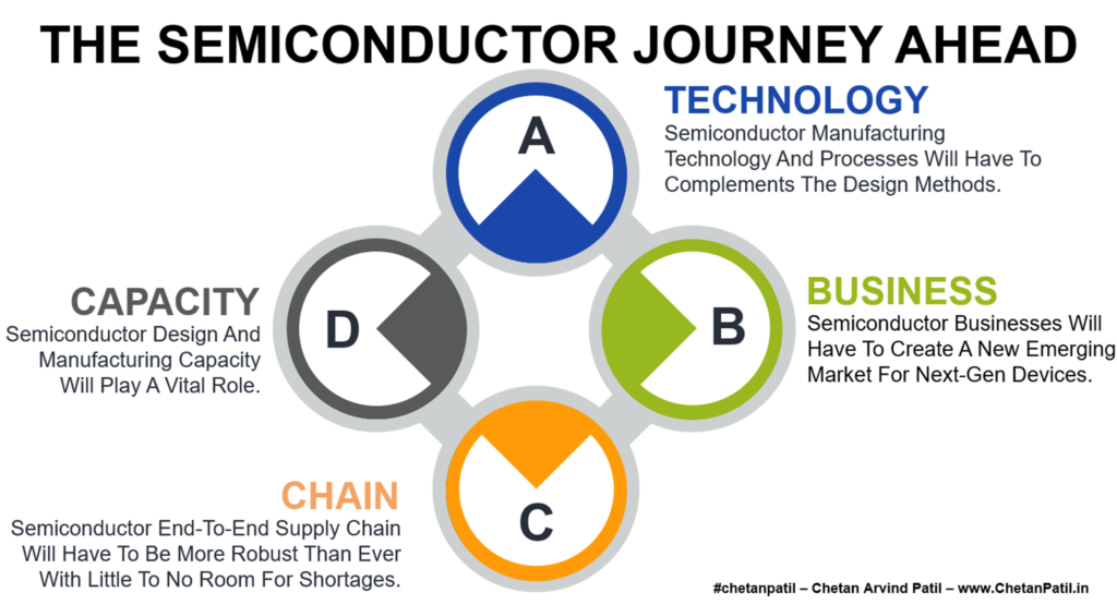
    Technology: The semiconductor manufacturing process will have to complement the design methodologies by enabling high-yielding error and defect-free processes.

    Business: Apart from the expansion of the existing market, semiconductor businesses will have to create a new emerging market for next-gen devices.

    However, achieving such a high target is not an easy task. It requires thorough planning from the industry level to the semiconductor business level. On top, this involves focusing on different aspects ranging from technological solutions to capacity building.

    In this regard, semiconductor design and manufacturing houses have been working hand in hand to come up with new technology-driven solutions and are also focusing on the capital required to enable new advanced solutions. The majority of the planning is still on paper and the next few years are crucial and will showcase whether the semiconductor industry will be able to expand its design and manufacturing capabilities to march toward the trillion-dollar market.


    Picture By Chetan Arvind Patil

    Apart from focusing on technology and business, semiconductor companies will require supply-level strategies to enable next-gen solutions. It means focusing on bringing more resiliency to the supply chain apart from building capacity for the semiconductor shortage-free world. Both demand in-depth planning for decades, if not years.

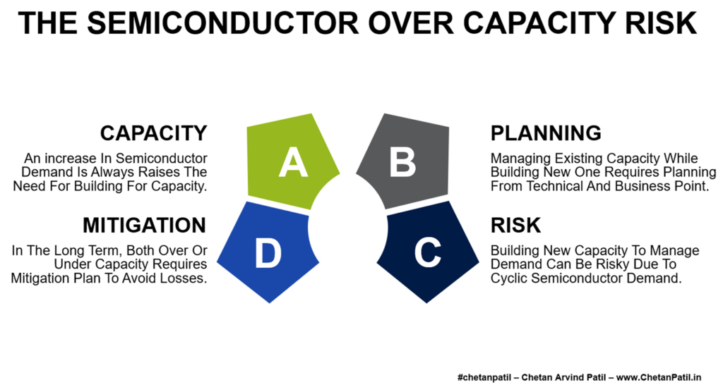
    The semiconductor shortage has sparked the debate to make resiliency to the supply chain and semiconductor capacity. Investments to address these two challenges have already been in the execution phase. However, there is also a risk if the demand goes down and the supply exceeds the requirement. The cost of not acting towards resolving the supply chain and capacity issues is far more than predicting the future.

    Chain: Semiconductor end-to-end supply chain will have to be more robust than ever with little to no room for shortages.

    Capacity: Semiconductor design and manufacturing capacity both are going to play a vital role in creating growth driven journey.

    Eventually, there is no magical process to enable the semiconductor industry to achieve high numbers by the end of the cade. it will all depend on how the market grows for the next decade and whether the plan the semiconductor business is executing will eventually help the semiconductor industry or not.


  • The Semiconductor And AI Adoption

    The Semiconductor And AI Adoption

    Photo by Jason Leung on Unsplash


    Artificial Intelligence (AI) driven by Machine Learning (ML) and Deep Learning (DL) has found its way into several industrial and consumer products. There is not a single high-tech solution that is not getting pitched as being AI-powered.

    AI also requires a silicon platform that can enable the training of a vast set of data apart to form accurate predictions using models. It will not be wrong to say that AI adoption is dependent on how efficient and error-free the silicon platform is.

    Market: AI-focused market is growing consistently and demands silicon that can enable faster decision making.

    Demand: AI-driven solutions create the need for silicon that require advanced semiconductor technologies.

    In 2022, there are already several AI-driven solutions utilizing the semiconductor capability to capture the market. Intel and AMD already have AI-focused XPUs that have enabled the computing industry to bring unique AI applications and services. Data-focused companies like Google, Amazon, and Microsoft have also spent years developing AI to help them understand consumer behavior faster than ever.

    The AI-driven market and the demand for silicon that can power such a solution will keep growing, this, in turn, will drive the need for more efficient XPUs.


    Picture By Chetan Arvind Patil

    Several emerging companies are focused on providing specialized XPU that can enable adaptive decision-making on the go. AlphaICs, Alphawave, Cambricon Technologies, Graphcore, and Groq are some examples. All of these are focused on creating a unique silicon platform to speed up the adoption of AI.

    Both enterprise and consumer markets demand AI-powered silicon that can cut down the cost and time to bring a new application to the market. As more consumers come online, the need for AI silicon will increase, and companies with the most bottleneck-free XPU solution will win the race.

    XPU: The demand for AI applications requires a silicon platform that can drive bottleneck data processing.

    Adoption: Smart silicon has already changed the AI race. As more elegant XPU silicon comes out, the adoption of AI-powered solutions will grow further.

    The semiconductor industry is already marching with advanced technology nodes and chiplets-driven advanced package technologies. Such advanced manufacturing solutions are perfect for powering next-gen AI chips. However, the cost and capital required to enable such a solution are very high. Thus the strategy to bring up the manufacturing capacity of advanced nodes for the AI world should be more robust than ever.

    The computing and semiconductor industries go hand in hand. As the need for consumer and enterprise-level AI-powered solutions grows, the adoption of AI chips will too, and semiconductors will (already are) play a pivotal role in decades to come.


  • The Semiconductor Value Flow

    The Semiconductor Value Flow

    Photo by Skye Studios on Unsplash


    Industries and companies worldwide are focused on creating value, without which it is not possible to survive the customer-driven market. The semiconductor industry is no different and has consistently added value over the last four decades.

    The value created by the semiconductor industry has enabled different other connected industries. It is evident based on the fact that semiconductor-focused solutions have become critical pillars for businesses that need innovative semiconductor-powered products.

    Value Flow: Solutions and products that take the semiconductor and other connected industries forward.

    To generate value consistently requires executing flawless strategy, which the semiconductor industry (mainly companies focused on product development) has carried out for decades. This value generation ranges from technology node, equipment, process development, package technology, raw material improvement, etc. There have been examples where such plans have failed, but the number of successful value creation-focused is considerably high.

    Segment: Creating segments that add value to the industry is the first step toward developing vital semiconductor value flow.

    Planning: Planning focuses on ensuring the development of segments leads to high-value creation, which demands consistent innovation.

    Creating value that drives the industry forward demands long terms focus and planning. It starts with focusing on segments that can add value. It can be new equipment, FABs to OSATs capacity building, new semiconductor devices, and several other sub semiconductor chain-focused segments. Along with a clear segment definition, robust planning is a must-have.


    Picture By Chetan Arvind Patil

    Creating segments and planning a long-term roadmap is a must-have for value flow. The other two parts of value flow creation are investment and learning.

    The investment focuses on building the capital and human resource to drive the segments that will bring the needed value to the semiconductor industry. And learning focuses on course correction required to ensure the value flow of new or existing domains does not go off track.

    Investment: Focuses on enabling required resources and teams that can constantly innovate the value flow.

    Learning: Capturing errors and failures to make necessary course correction is vital to creating a robust value flow.

    Value flow has become an integral part of the semiconductor industry. Mainly due to the growing dependency on semiconductor products. Such a dependency demands highly focused value flow management. If not done correctly, it can often lead to situations similar to semiconductor shortages.

    The semiconductor industry is bound to grow in the coming decades. It is valid both from market size and numerous products that will get manufactured. Value flow needs to be more robust to achieve these goals, and the semiconductor industry thus will have to keep finding new avenues to make the new and existing value flow more resilient and innovative.


  • The Need To Open Source Semiconductors

    The Need To Open Source Semiconductors

    Photo by Shahadat Rahman on Unsplash


    Semiconductor end-to-end product development is a highly complex process. The majority of these processes are also proprietary. Developing a proprietary process is vital as it allows companies to bring innovation and never-seen-before products and solutions, which in the long term drive market position and revenue. However, opening up certain parts of the process is also vital for knowledge building.

    In the software industry, there have been numerous open source solutions. Doing so has only benefitted the software industry, which has enabled the development of new software-driven ideas. On top, it has powered a collaborative environment that drives knowledge building.

    In comparison, the semiconductor industry is far behind. Open hardware has been around, but it has not helped the semiconductor industry. The main reason is the focus on assembling rather than the design of semiconductors or the building blocks that make up the semiconductor chips.

    Ideas: Open sourcing certain aspects of semiconductor design and manufacturing will drive the development of new ideas.

    Knowledge: Students and academia will get a lot from open-source (FET level) semiconductor-focused information that can enable new research activities.

    The benefits of open sourcing specific information are many. It allows anyone to learn and build from scratch. In this direction, semiconductor-driven companies have opened up Process Design Kit (PDK), a step in the right direction. PDKs allow individuals to take a deep look into the transistor-driven systems. If there are areas of improvement (power, performance, thermal, and so on), then a new PDK can be released (open sourced). It can then create a chain reaction of process developments. Long-term benefits will be the knowledge and idea-sharing that such continuous improvement will drive.

    Open-sourcing PDK is a welcome move. However, several other information and details can be shared (without impacting internal research). So that anyone with a focus on semiconductors can turn the open source into new solutions for the semiconductor industry.


    Picture By Chetan Arvind Patil

    Open-sourcing in the software industry has shown long-term benefits. It ranges from releasing new software tools to programming languages. In many cases, it has also led to even launching companies.

    However, open-source does come with a certain level of risk, whereby the companies have to balance what can and cannot be shared. This problem quadruples in the semiconductor industry as the time and capital required to develop new solutions are high, and not possible to open-source all the information.

    The semiconductor industry thus has to find a middle ground by at least open sourcing some of the old technologies which do not see much industry-wide development. Doing so will allow students and entry-level positions to develop skills by leveraging the open-sourced details of the technology node or the package technologies.

    Tools: Developing tools for silicon development is a complex process. Open-sourcing some libraries on the process and package size can go a long way in enabling open-source tool development.

    Collaboration: Open source has always enabled a collaborative approach that allows the development of ideas and processes. A similar impact is possible in the semiconductor industry.

    Open-source collaboration can also enable the development of next-gen FET devices. So far, there have been no attempts to collaborate (via an open-source model) on FET devices. Doing so might enable the industry with ideas that can provide a way forward toward the More-Then-Moore era.

    While the industry is gearing up for increasing semiconductor design and manufacturing (worldwide), the focus should also be on how to bring in more collaboration-driven innovation. The standardization approach has also helped but to a certain extent.

    In the long-term, the focus should also be on open-sourcing specifics of each of the end-to-end semiconductor design and manufacturing. It will not only go a long way in attracting new talents but also can bring several innovative ideas.


  • The Process Of Building Semiconductor Ecosystem

    The Process Of Building Semiconductor Ecosystem

    Photo by Shubham Dhage on Unsplash


    The end-to-end semiconductor design and manufacturing are dependent on the ecosystem. It is evident from the regions that have become a pillar of the semiconductor industry. These regions have grown steadily for decades while creating business and employment opportunities.

    Developing a semiconductor ecosystem is not an easy process. It demands time, resources, and capital, which are not easy to come by together. Existing semiconductor ecosystems have been around for more than two to three decades and thus have become a benchmark for the upcoming semiconductor regions.

    New regions that want to attract semiconductor businesses should focus on creating a semiconductor ecosystem. Doing so requires following a set process to bring together different building blocks of the semiconductor industry. These fundamental blocks create a platform that allows semiconductor-focused businesses to thrive for decades to come.

    Core: Focus on developing the region for one specific type of semiconductor business. For example, focusing on semiconductor design or manufacturing is far better than focusing on both.

    Support: Apart from developing core competency, also build a supportive environment that supports and helps the growth of different semiconductor businesses.

    The semiconductor ecosystem development starts with the core focus. Focus on one solution rather than focusing on all the segments of semiconductors. It is how some of the semiconductor ecosystems in Taiwan (manufacturing), the EU (equipment), Japan (material and equipment), China (assembly), and the USA (design) started and are now (or already have) becoming ecosystem with multi-segment semiconductor business.


    Picture By Chetan Arvind Patil

    The continuous growth of the semiconductor ecosystem demands a supportive environment. Companies within a semiconductor ecosystem should thus focus on cross-collaboration. Such an approach allows the development of a new type of semiconductor technology.

    Focus: Long-term focus is required by enabling collaborative culture that allows the flow of innovative ideas.

    Infrastructure: Basic infrastructure developed by public bodies goes a long way in making a robust semiconductor ecosystem.

    Public bodies also play a vital role in creating a semiconductor ecosystem. It ranges from providing adequate infrastructure to laying out policies to make it easy to do business. Education infrastructure is also critical for the free flow of talent that eventually drives the semiconductor ecosystem forward. There are already several examples whereby the proximity of a university powered the overall growth of the semiconductor business.

    As the race to attract semiconductor businesses to set up the design to manufacturing houses speeds up, the case to create a semiconductor ecosystem will grow and might be a de-facto way of developing regions.


  • The Ever-Increasing Share Of Semiconductor In Automotive

    The Ever-Increasing Share Of Semiconductor In Automotive

    Photo by Chris Liverani on Unsplash


    Automotive has always been an integral part of day-to-day life. Worldwide, billions of people drive vehicles, and the goal is the same: reaching the next destination safely and on time. Achieving this goal is only possible due to the different features and components that come together to enable an end product that can zoom safely.

    A lot of effort goes behind the scenes to meet customer demand and automotive safety requirements. Any given vehicle demands thousands of tiny parts procured (or manufactured) from different vendors. Eventually, all these components need to work synchronously to provide the safest ride possible.

    Safety: Silicon products enable real-time decision-making, a must-have feature for maintaining the standard of automotive safety.

    Autonomy: Autonomy focuses on assisting safe rides, and it requires error-free silicon products that can work in any conditions.

    In this line, one of the vital part, whose share in automotive products have increased steadily year on year, is a semiconductor. Semiconductors are part of every vehicle out on the road. These tiny devices (packaged as silicon chips) enable different features.

    In the last decade alone, the number of semiconductor products in modern vehicles has increased by 10x. Such a drastic increase in demand is majorly due to new features apart from the need to make every ride a safe and enjoyable one. It is also evident from the growing demand for automotive-focused semiconductor solutions, which will increase further with the adoption of more alternate-fuel solutions that will increase the share of semiconductors in next-gen vehicles.


    Picture By Chetan Arvind Patil

    One of the drastic changes in the automotive industry is the centralization approach. CAN-based solutions were already available for decades. However, the availability of more reliable XPU based solutions has pushed the centralization towards a new era and is transforming automotive into a computer on the wheels. Thus, opening up the market for companies that never focused on automotive segments.

    It also implies that the thermodynamics of automotive products is changing and slowly becoming semi-dynamics. In the semi-dynamics world, the decision is driven by silicon products while also working alongside the traditional thermodynamic system. Such reliance will grow further, already has, with alternate-fuel, hybrid, and electric approaches.

    Centralization: Automotive products are getting loaded with high-performance computer chips, which are more centralized than ever before.

    Features: New features require new silicon products that focus on improving customer experience by enabling highly reliable products.

    Even though automotive semiconductor demand is increasing, it will not be easy for emerging companies to make the most of the growing market. The reason is the safety, quality, and reliability standards that automotive products demand. It is not only time-sensitive but also capital intensive. Still, there are promising upcoming automotive semiconductor-focused emerging companies making the mark in the market. However, such companies will face stiff competition from the existing established players.

    The next decade will be an exciting one for automotive semiconductor companies. The focus will be on highly dynamic, safe, and reliable semiconductor-driven products that will enable a new ear of transforming mobility.


  • The Semiconductor Over Capacity Risk

    The Semiconductor Over Capacity Risk

    Photo by Taylor Hammersla on Unsplash


    Semiconductor capacity has been the most talked-about topic due to the semiconductor shortage. Companies and countries are upgrading or building semiconductor manufacturing to cater to ever-increasing demand. However, simply increasing the semiconductor capacity is not the answer and often comes with several techniques to business challenges.

    The technical challenge involves deciding on the technology-node and package technology to focus on, which is not an easy decision and requires an end-to-end view of how the market will evolve and which technology will be crucial. Yield and throughput also play a role. On top of all this, the technology (lithography as an example) equipment required should work as expected. More so when the new capacity focuses on advanced semiconductor solutions.

    Capacity: Building new semiconductor manufacturing capacity is not always the answer to capacity constraints. It can solve the problem in the short term. As a robust strategy, a more predictive, not reactive approach is suitable.

    Planning: Near-accurate prediction of how the industry will evolve is required. It enables accurate planning of how and when to build new capacity apart from when to upgrade the existing one.

    From the business perspective, the challenge is justifying the capital expenditure against the return on investment. In semiconductor manufacturing, 100% utilization is key to achieving a faster break-even point, and at the same time, it is not always possible to achieve such throughput. It is where government incentives come into the picture and act as a catalyst to drive the positive margin gain year on year.

    Even after overcoming the technical and business challenges, there is always the risk of building new capacity, which is driven by how the market demand evolves in years to come and how it will impact the manufacturing business in the long term.


    Picture By Chetan Arvind Patil

    Historically, the semiconductor business has always followed a cyclic nature, whereby the supply and demand are adjusted. This adjustment then triggers a round of discussion on expanding manufacturing capacity. By the time capacity comes up, the market demand may go down, and this can cause lower than expected orders for specific semiconductor silicon, which can derail the ROI plans of the given semiconductor manufacturing facility.

    Tackling such unknown scenarios is not straightforward. Thus, it is vital to have a full-proof risk mitigation plan. An ideal risk mitigation plan focuses on what-if scenarios and adapts to how the market changes. The manufacturing facility adapts to the requirement while maintaining the path towards break-even. It can demand continuous capital and is a must-have to run a successful semiconductor manufacturing facility.

    Risk: Expanding capacity without planning is a risk-driven approach. There needs to be a risk management strategy to mitigate any unknown event that can impact the planning of capacity building or upgrading.

    Mitigation: Mitigation strategy for capital-intensive semiconductor manufacturing is a big challenge. An adaptive approach that focuses on the market scenarios is a must-have.

    On paper, such planning is good but equally hard to implement. The reason is the inability to adapt semiconductor manufacturing planning without adding the time factor, which is needed to change the future course of any production facility.

    As new semiconductor FABs and OSATs come up, the question industry should ask is whether it is preparing itself for an over-capacity scenario and what is the mitigation plan when the market swings.


  • The Semiconductor Hurdles For Inspection

    The Semiconductor Hurdles For Inspection

    Photo by L N on Unsplash


    Semiconductor products often fail, and finding the root cause thus becomes a critical process. More so, when the product is already in production.

    Failure and root cause analysis are vital steps towards finding issues with the semiconductor product. Doing so requires an inspection process that allows engineers to look inside the chip.

    Several advanced equipment and technologies (SEM and beyond) can provide an in-depth view of what is happening inside the chip. The hurdles thus are not the availability of technology required to drive failure analysis. The real challenge is the complexity (silicon level) that the advanced design and manufacturing brings to enable failure analysis.

    Complexity: Growing transistor count increases the die level complexity, which brings difficulties to perform failure analysis without investing more than the required time, resources, and capital.

    Failure: During failure analysis (in the majority of the cases), it becomes difficult to narrow down the root cause for highly complex (3nm and lower) products. Advanced equipment does help, but not without investing a lot of time and cost.

    Overcoming different inspection hurdles is a vital step towards a fast resolution of why the product failed. At the same time, the growing design complexity of semiconductor products (coupled with different package technologies) is leading to constant upgrades of labs that enable such analysis and leading to the high cost of finding the defects in the product.


    Picture By Chetan Arvind Patil

    The fundamental process when carrying out failure analysis is the localization of defects. Doing so requires semiconductor products to run through several inspection steps, and it often requires looking at every layer. Biasing process helps, but it requires skilled engineers with years of experience to handle the inspection tools to find areas of concern within a given chip.

    Defect: Year on year, the localization of defects during the failure analysis is getting costlier and time-consuming. All of this leads to constant upgrades of equipment apart from the training of engineers.

    Cost: The cost of inspection to capture the failures is increasing due to the need to constantly upgrade labs apart from the time required to find defects in the highly complex products with advanced technology nodes. Solutions like do SEM are helpful but are also high on cost.

    Today’s advanced semiconductor product utilizing the latest technology node often comes equipped with billions of devices. Inspecting such devices is certainly not an easy task. More so, when the goal is to quickly root cause silicon-level issues.

    The importance of inspection as part of a semiconductor product (in case of failures) will only grow with the growing number of transistor counts. It is thus vital to focus on optimizing the process to perform failure analysis so that the operating cost is reasonable while also bringing skilled engineers who can efficiently carry out inspection-driven failure analysis.


  • The Cross Collaboration And Standardization Across Semiconductor Industry

    The Cross Collaboration And Standardization Across Semiconductor Industry

    Photo by Nick Fewings on Unsplash


    There are several parts to semiconductor product development, and without cross-industry collaboration and standardization, it is impossible to move forward (next-gen solutions).

    Collaboration and standardization have triggered several innovative solutions that have only taken the semiconductor industry forward. These strategic approaches come in different forms. Some are between two or more semiconductor-focused companies, many driven by consortiums of several companies (semiconductor and non-semiconductor). Irrespective of the approach, the focus is to bring new semiconductor technologies.

    Collaboration Benefits: It fosters the environment where one or more companies can share the knowledge to enable next-gen devices that can create future markets while expanding the current one. Examples of such collaboration are many. Collaboration between XPU developers and non-XPU developers is one. The reason one relies on the other and has to follow a collaborative approach to ensure the end products (desktops, laptops, smartphones, etc.) work flawlessly.

    Standardization Benefits: One of the impacts of standardization is that it allows product development knowledge sharing irrespective of the resources and capital any given company has. An example of this can be all USB or Wi-Fi-driven silicon solutions as it follows a standard protocol and empowers companies to build on top of it. Recently announced Universal Chiplet Interconnected Express is also one such example.

    The two positive impacts of collaboration and standardization are knowledge sharing and learning. Given how high-tech the semiconductor industry is, the knowledge transfer and learning approach enables a thriving business and expands the reach of semiconductor products.

    Knowledge: Sharing technical knowledge that helps the industry move forward is only possible via active collaboration.

    Learning: Capturing learnings based on old solutions allows the development of new solutions for the emerging market, which also requires standardization and continuous collaboration.

    The semiconductor industry-wide standards from the past decades have already shown the world several innovative solutions. Majority of which came out of active collaboration. It is also true that no given semiconductor company can thrive without active cross-industry partnerships. More so when the devices today require multiple and different types of solutions.

    In the end, the goal of collaboration and standardization in the semiconductor industry is to drive a new age of innovation, something the global semiconductor ecosystem has done very well for the last four to five decades.


    Picture By Chetan Arvind Patil

    Apart from the technical benefits, the two other vital impacts of collaboration and standardization are the expansion of business via existing or near markets along with the ability to launch next-gen devices. It is evident from the fact that today’s smart devices that were only possible due to the active collaboration of different types of semiconductor companies.

    Several of these strategic collaborations are proprietary. Which is also required to ensure the different businesses can create a niche market for themselves. On another side, there have been several open collaborations. All of which have moved the industry forward and have allowed design and manufacturing companies to come up with solutions to power next-gen solutions.

    Business: Different types of semiconductor businesses benefit from standardization as it creates a level playing field on the top of which companies can develop new solutions.

    Next-Gen: Emerging solutions (chiplets and photonics as an example) are only possible via industry-wide standardization. Otherwise, the speed of adoption will be slow.

    Active collaboration is also key to bringing new solutions forward. Semiconductor lithography solution is one such example. It has been able to leap forward only due to the long-term strategic planning and focus. Some of which have also been with academia.

    As the need to push for More-Then-Moore solutions grows further, the importance of semiconductor collaboration and standardization will grow too and make the semiconductor ecosystem more advanced than ever before.


  • The Growing Reliance Of Semiconductor Industry On Software

    The Growing Reliance Of Semiconductor Industry On Software

    Photo by ThisisEngineering RAEng on Unsplash


    Software is the backbone of several industries, including semiconductor. Several (maybe all) semiconductor activities cannot work without a software solution and are valid for several key stages like design, manufacturing, supply chain, and many more.

    This growing reliance on several stages is the primary reason it has become vital to utilize the best solution for all the stages of semiconductor product development. Doing so enables defect-free and error-free solutions for the end customers.

    The advancement in software tools has allowed the semiconductor industry to lower the time to market. As more advanced semiconductor technologies get deployed, the importance of developing faster and more accurate software will grow further and increase the reliance of the semiconductor industry on software solutions.

    Automation: Automated software solutions plays a critical role in capturing defects and errors during design or manufacturing stages.

    Time To Market: Software speeds the process of developing and launching semiconductor products. The reason is the ability to simulate and capture all the errors before products go to the customer.

    One key feature of the software is automation. It speeds up designing and also ensures defects get captured ahead of time. On another side, the software is powering the designing process of highly complex products without human interference.

    In the long run, such solutions may or may not work. However, raises questions of how much more software solutions can do (concerning design and manufacturing) and how it will impact the semiconductor industry.


    Picture By Chetan Arvind Patil

    Apart from semiconductor product development (design and manufacturing), the software also plays a vital role in semiconductor information management. It includes capturing and storing all the required data for a very long time.

    Software solutions around information and data management have been around for decades. However, the growing data complexity and the need to capture/process the data faster is leading bottleneck’s in the software solutions themselves. It has raised the demand for a new generation of software solutions to pull the information faster than ever.

    Management: Information management is a part of semiconductor product development and demands easy-to-use software solutions.

    Life Cycle: Managing product information demands long-term software-powered data storage and retrieval.

    As the need to reduce the time to market grows, the demand for software-driven automation will grow more. Semiconductor-focused software automation has been in place for several years. However, the market needs to enable new types of silicon products for the emerging market is demands novel ways to design and manufacture.

    All these requirements will further grow the reliance of the semiconductor industry on software and thus presents an opportunity to innovate software solutions to meet growing semiconductor industry demand.