- Hosted By: IEEE Student Branch, DYPIU, And Supported by IEEE Young Professionals (YP) of The D Y Patil International University
- Location: Virtual/Online
- Date: 8th November 2025
Blog
-

Shaping The Future: Pathways And Possibilities In Semiconductor Engineering
-

Semiconductor Test Handlers – Driving Efficiency And Reliability in High-Volume Production
Published By: Electronics Product Design And Test
Date: November 2025
Media Type: Online Media Website And Digital Magazine -

The Case For Energy-Aware Semiconductor Lithography
Image Generated Using DALL·E
Rising Energy Burden Of Lithography
Lithography has become one of the most energy-intensive stages in the fabrication of wafers. As fabs push to 2 nm and below, every additional patterning layer increases electricity demand and associated CO₂ emissions. Industry projections now indicate that wafer-fab emissions will exceed approximately 270 Mt CO₂e by 2030, primarily from equipment-driven loads. Fabs cannot treat lithography power as a fixed cost anymore.
High-NA EUV, expected to be widely deployed in high-volume environments, delivers the resolution needed for advanced logic. However, it also increases per-tool power requirements, precisely the kind of “performance/energy ↑” tradeoff that sustainability teams are trying to mitigate. This imbalance is the reason lithography is now being singled out in sustainability roadmaps.
What “Energy-Aware” Really Means
Energy-aware lithography integrates power consumption as a design and operational variable within the patterning process, alongside resolution, critical dimension control, and throughput. Instead of viewing electricity as a fixed cost, it measures kWh per wafer and CO₂ per layer as core performance metrics. Each exposure plan and dose setting is evaluated for both imaging fidelity and energy efficiency, shifting lithography from precision alone to precision with purpose.
At the fab level, energy awareness spans scanner design, standby control, and load balancing across exposure tools. It links process control with power management, allowing for the precise achievement of exact yield and overlay targets with reduced energy consumption. In this framework, sustainability becomes an engineered outcome rather than an afterthought.

Image Credit: IEA
Emerging Data From Recent Research
Recent years have seen semiconductor research institutions and equipment makers quantify lithography’s energy and carbon footprint with far greater precision. This shift from broad sustainability targets to verifiable metrics such as energy per wafer, kilowatt-hours per layer, and carbon dioxide equivalent per exposure has redefined how efficiency is measured.
Organizations such as imec, ASML, and TSMC now publish data showing measurable progress in reducing power consumption across both process and equipment levels, aligning with the 2024 IRDS Environmental Chapter, which calls for quantifiable energy tracking throughout semiconductor manufacturing.
At the same time, policy frameworks such as NIST’s 2024 environmental assessment and SRC’s sustainability initiatives have recognized tool-level efficiency as a direct lever for emission reduction. This alignment between research, industry reporting, and regulatory guidance represents the first coordinated movement toward energy-transparent lithography, where every exposure and patterning decision is tied to a measurable energy outcome.
Paper Title Year And Paper Link Summary And Relevance Toward Lifelong-Sustainable Electronic-Photonic AI Hardware 2025
arXivHighlights that for cutting-edge chips the embodied carbon (including lithography/EUV) is growing even as operational efficiency improves. Useful for framing lithography’s sustainability burden. Carbon Per Transistor (CPT): The Golden Formula for Sustainable Semiconductor Manufacturing 2025
arXivPresents a quantitative model of semiconductor fabrication carbon footprint, highlighting that lithography (with other front-end steps) dominates wafer-fab emissions. Can we improve the energy efficiency of EUV lithography? 2024
arXivDirectly addresses EUV lithography power consumption and suggests routes to reduce source power by an order of magnitude, highly relevant for your lithography-energy theme. Modeling PFAS in Semiconductor Manufacturing to Quantify Trade-offs in Energy Efficiency and Environmental Impact of Computing Systems 2025
arXivWhile focused on PFAS (materials), this paper also touches on patterning complexity (incl. lithography) and embodied carbon/material trade-offs, useful to show the broader sustainability context. Carbon Connect: An Ecosystem for Sustainable Computing 2024
arXivDiscusses large-scale manufacturing, including semiconductor fabs’ electricity usage (comparable to datacenters) and mentions extreme ultraviolet lithography in that context. How purity reshapes the upstream materiality of semiconductor manufacturing 2025
arXivAddresses supply-chain/material dependencies for lithography (e.g., neon/argon gases for excimer lasers) and helpful to show indirect energy/material burdens tied to lithography. Recent studies from imec, ASML, and TSMC, supported by analyses such as Shintake (2024) on EUV power reduction and ElSayed et al. (2025) on carbon-per-transistor metrics, show a clear shift in how lithography energy is being addressed. The emphasis has moved from large facility upgrades to tool- and process-level optimization, where adaptive standby control, exposure planning, and dose tuning yield immediate reductions in power use.
Together, these works demonstrate that lithography energy is now a quantifiable engineering parameter. Integrating power metrics into process control and equipment specifications turns sustainability into a driver of performance, advancing the concept of truly energy-aware semiconductor manufacturing.
Toward A Metric Of Energy Transparency
Latest developments across the industry have also highlighted a growing focus on the transparent reporting of lithography energy use. ASML has disclosed that its NXE:3600D EUV systems consume about 7.7 kilowatt-hours per exposed wafer pass, offering a concrete reference point for equipment-level efficiency.
IMEC’s modeling work indicates that lithography and etch together contribute over 40 percent of Scope 1 and 2 carbon emissions at advanced logic nodes, emphasizing where process-level optimization delivers the most significant impact. TSMC’s EUV Dynamic Power Saving Program further demonstrates operational transparency by achieving a 44 percent reduction in peak power and projecting 190 million kilowatt-hours in energy savings by 2030.
These examples collectively point toward a future where lithography energy is treated as a measurable parameter rather than an indirect cost. Adopting standard metrics, such as kilowatt-hours per exposure or carbon-equivalent per layer, would allow fabs and equipment suppliers to benchmark their performance and optimize power alongside yield and throughput.
Energy transparency at this level establishes efficiency as a shared engineering objective across the semiconductor ecosystem.
-

The Semiconductor Yield Management Systems From Data To Intelligence
Image Generated Using DALL·E
The Yield Economic Of Semiconductor Manufacturing
Yield is the percentage of functional chips produced per wafer and is the foundation of semiconductor economics. Every wafer starts as a costly investment in materials, equipment time, and process precision.
When more dies on that wafer, work perfectly, and each functional chip costs less to produce, margins and profitability improve directly.
At advanced technology nodes, where wafer costs can exceed tens of thousands of dollars, even a 1% yield gain can translate into millions in savings. This is why yield is not just a technical metric. It is a financial one. High yield lowers cost per die, improves gross margin, and enables companies to price products more competitively.
As process complexity grows, yield becomes harder to maintain. Each new node introduces tighter tolerances and new failure modes, linking technical precision and financial outcome more closely than ever.
In essence, yield is the quiet bridge between engineering excellence and economic success and the factor that decides whether innovation becomes profit.
How Data-Driven Yield Management System Have Evolved
Yield management has advanced from manual inspection to intelligent, data-driven automation, a transformation shaped by decades of progress in data collection, analytics, and system integration. As semiconductor processes grew more complex, traditional visual checks and spreadsheets could no longer keep pace with the precision required to sustain competitive yields.
Modern fabs now deploy Yield Management Systems (YMS) that integrate real-time data, advanced analytics, and machine learning to transform yield from a passive metric into a predictive, actionable insight. The table below outlines this evolution:
Era Key Characteristics Data Capabilities Challenges Manual Era
(1980s–2000s)Visual inspections, manual SPC charts, and basic defect tracking. Limited data collection and offline analysis using spreadsheets. Slow feedback loops, poor traceability, reactive response. Advanced Era (2000s–2020s) Automated SPC, digital defect logging, and integrated tool monitoring. Centralized data storage with faster trend analysis and limited automation. Limited predictive analytics, partial integration across systems. Automated Era (2020s–Present) Real-time data acquisition from MES, metrology, and sensors. Full integration with cloud computing, AI/ML-based yield prediction, and cross-fab traceability. Managing large data volumes, ensuring interpretability of AI results. In the early decades, engineers tracked yield using simple control charts and manual logs. These methods provided limited visibility and slow feedback, often revealing problems only after yield had already been lost.
As wafer complexity increased, manual processes could no longer scale. Semiconductor manufacturers began integrating automated data collection and Statistical Process Control (SPC) into production lines, enabling faster detection of process drifts and systematic analysis of defect trends. This marked the transition from reactive monitoring to structured yield control, where data became central to manufacturing stability.
Feature Description Purpose And Impact Data Acquisition Layer Real time interface with MES, metrology, and inspection tools Enables continuous monitoring and instant process feedback Statistical Process Control (SPC) Automated Cp Cpk tracking, control charts, and deviation alerts Ensures process stability and early defect detection Fault Detection and Classification (FDC) Algorithms identify and categorize process or tool abnormalities Prevents downtime by enabling predictive maintenance Machine Learning Analytics Uses PCA, random forests, and anomaly detection for yield prediction Detects subtle variations that impact yield before failure occurs Visualization Dashboards Unified display of yield, WAT, and test data across tools and lots Improves decision speed and cross functional collaboration Today, modern fabs operate within a fully connected analytics ecosystem. Yield Management Systems now merge real-time data acquisition, advanced visualization, and machine learning to predict yield excursions before they occur.
These systems link data from metrology, inline inspection, test, and equipment health monitoring into a unified view, empowering engineers to act proactively rather than retroactively. This evolution has redefined yield from a diagnostic indicator into a strategic, data-driven performance metric.
Cost, ROI, And The Business Of Yield
Deploying a Yield Management System involves both technical and financial commitments. Semiconductor manufacturing involves substantial capital costs, including tools, cleanrooms, and data infrastructure.
Implementing a YMS adds software licensing, integration, and personnel training expenses, but it also transforms how that investment performs.
By reducing variability, minimizing scrap, and accelerating problem resolution, yield improvements translate directly into lower cost per die and more substantial gross margins. Even a slight percentage increase in yield at advanced nodes can generate multi-million-dollar savings across high-volume production.
The return on investment extends beyond immediate cost reduction. Higher yields shorten time-to-market, improve equipment utilization, and stabilize supply. These gains compound over a product’s lifecycle, improving financial predictability and enabling greater reinvestment in research and development.
In essence, a well-implemented Yield Management System becomes not only a quality tool but a profit multiplier, turning data intelligence into sustained economic advantage.
The Transition From Automation To Intelligence
Semiconductor yield management is entering a new phase where automation alone is no longer enough. The focus is shifting toward systems that think, learn, and respond in real time. Yield Management Systems are evolving to integrate machine learning, hybrid cloud data platforms, and inline process feedback.
These advancements allow fabs to identify deviations earlier, make predictive corrections, and maintain consistent output even as manufacturing complexity continues to rise.
The future of yield management lies in intelligence that is both adaptive and interpretable. Systems will not only detect issues but also understand why they occur and recommend precise corrective actions. This transformation will redefine yield as a measure of insight rather than output.
In this intelligent era, yield becomes a continuous learning loop, linking every wafer, process, and decision into a unified path of improvement and resilience.
-

The Semiconductor Workload-Aware Architecture
Image Generated Using DALL·E
From Node-Centric To Workload-Centric
For more than five decades, semiconductor innovation revolved around a single pursuit: shrinking transistors. Each new process node promised higher density, lower cost per function, and faster circuits. This node-centric model powered the industry through its golden era, making smaller equivalent to better. As the limits of atomic scale physics approach, that once predictable equation no longer holds.
Progress is now measured by workload alignment rather than by node advancement.
The key question for designers is not how small the transistors are but how well the silicon reflects the behavior of the workload it runs. This marks a fundamental transformation from process-driven evolution to purpose-driven design.
To understand how this transformation unfolds, it is essential to define what workload awareness means and why it changes the way semiconductors are built.
The Concept Of Workload Awareness
Workload awareness begins with the recognition that computation is not uniform. Each class of workload, such as neural network training, radar signal analysis, or camera data processing, shows distinct patterns of data flow, temporal locality, and parallelism. Recognizing these patterns allows designers to shape architectures that match computation to structure instead of forcing different workloads through one standard design.
Traditional architectures focused on generic performance through higher frequency, larger caches, or more cores. Such approaches often waste energy when the actual bottleneck lies in memory bandwidth, communication latency, or synchronization overhead. A workload-aware design begins with profiling. It identifies how data moves, where stalls occur, and how operations scale in time and energy.
Workload Type Key Characteristics Architectural Focus Example Design Responses AI Training Dense linear algebra, large data reuse, high bandwidth demand Compute density and memory throughput Tensor cores, high bandwidth memory, tiled dataflow AI Inference (Edge) Low latency, sparsity, temporal reuse Energy efficient compute and memory locality On chip SRAM, pruning aware accelerators Automotive Real time, deterministic, mixed signal Low latency interconnect, redundancy Lockstep cores, time sensitive networks Signal Processing Streaming data, predictable compute patterns Deterministic pipelines, throughput balance DSP arrays, low latency buffers Industrial Control Small data sets, long lifetime, low cost Reliability and integration Mature nodes, embedded NVM This awareness reshapes design philosophy. Instead of optimizing transistors alone, engineers now optimize data pathways, compute clusters, and memory placement based on the workload characteristics.
In practical terms, this means choosing architectural topologies such as mesh fabrics, matrix engines, or local scratchpads that mirror the natural behavior of the workload.

Image Credit: Workload-Aware Hardware Accelerator Mining for Distributed Deep Learning Training
The Architectural Shifts
The move from node-centric to workload-centric design is transforming semiconductor architecture. Efficiency now depends on how well compute, memory, and packaging align with the behavior of each workload rather than how advanced the process node is.
This transformation spans the entire hierarchy. Every layer, from compute logic to system orchestration, must now reflect how data flows and where energy is spent.
Key Architectural Shifts
- Compute: Transition from monolithic processors to heterogeneous clusters with domain-specific accelerators such as matrix engines, DSPs, and control cores.
- Memory: Focus moves from capacity to proximity. Data is placed closer to the compute using high bandwidth memory, embedded DRAM, or stacked SRAM.
- Packaging: The package becomes an architectural canvas. Two-and-a-half-dimensional and three-dimensional integration combine logic, memory, and analog dies from multiple nodes.
- Interconnect: Movement from fixed buses to scalable low-latency fabrics using silicon bridges, interposers, and emerging optical links.
- System Orchestration: Compilers and runtime software allocate resources dynamically, adapting to workload behavior in real time.
These shifts mark a deeper alignment between physical design and computational intent. Each layer now collaborates to express the workload rather than merely execute it.
When compute, memory, and packaging act as a unified system, hardware becomes adaptive by design. This forms the core of the workload-aware architecture and sets the stage for a new scaling model driven by purpose instead of geometry.

Image Credit: Towards Efficient IMC Accelerator Design Through Joint Hardware-Workload Co-optimization
Workload-Based Scaling Law
For many decades, semiconductor progress followed a simple path: smaller transistors meant faster, cheaper, and more efficient chips. That rule of geometric improvement, often described as Moore’s Law, guided every roadmap. As scaling reaches physical and economic limits, the performance gains once guaranteed by smaller nodes have diminished.
Today, most power is spent moving data rather than switching transistors, and actual efficiency depends on how well the architecture aligns with the workload itself.
Workload-based scaling redefines progress as performance per watt per workload. It evaluates how compute, memory, and interconnect cooperate to execute a specific data pattern with minimal energy. A well-tuned architecture at a mature node can outperform an advanced node if it matches the workload precisely.
This marks a transition from geometry to behavior, from transistor count to data awareness. Future leadership in semiconductors will belong to those who design not for smaller features, but for smarter alignment between computation and workload intent.
-

The Need For Silicon To Become Self-Aware
Image Generated Using DALL·E
What Is Silicon-Aware Architecture
As chips approach atomic dimensions, every region of silicon begins to behave differently, shaped by fluctuations in voltage, temperature, stress, and delay. Traditional design methods still rely on fixed timing corners and conservative power margins, assuming stable and predictable behavior.
At three nanometers and below, this assumption breaks down. Modern workloads in artificial intelligence, edge computing, and automotive systems operate under constantly changing physical and electrical conditions. To sustain both performance and reliability, silicon must evolve beyond precision into perception. It must know its own state and react intelligently to it.
A silicon-aware architecture is the structural basis for this evolution.
It represents a chip that not only executes logic but also perceives its own electrical and physical behavior in real time. Embedded networks of sensors, telemetry circuits, and adaptive control logic create continuous feedback.
The chip measures temperature, voltage, and aging, interprets the data internally, and fine-tunes its operation to maintain stability and efficiency. In doing so, the silicon transforms from a passive substrate into an active, self-regulating system capable of sustaining peak performance under diverse and unpredictable workloads.
Adapting To Workload Reality
Artificial intelligence workloads have redefined how silicon is stressed, powered, and utilized. Unlike conventional compute tasks that operate within predictable instruction flows, AI inference and training involve highly dynamic activity patterns. Cores experience extreme bursts of power consumption, rapid switching between memory and logic, and localized thermal buildup.
These workloads create transient peaks in current density that can exceed traditional design margins by several times. A static chip designed with fixed voltage and frequency limits cannot efficiently manage such fluctuations without wasting energy or compromising reliability.
Adaptive Function Challenge In AI Workloads Traditional Limitation Silicon-Aware Advantage Thermal Regulation Localized hotspots in dense compute clusters Global throttling reduces overall throughput Localized sensing and targeted bias control Power Delivery Rapid current surges during tensor operations Static voltage rails with limited response On-die regulation based on real-time telemetry Reliability Aging High stress cycles on interconnects and transistors Static lifetime derating Predictive control extending operational lifetime Workload Distribution Uneven utilization across cores Coarse scheduling by firmware Autonomous, per-region load balancing A silicon-aware architecture introduces a path forward by allowing the chip to interpret its own activity and respond within microseconds.
Through embedded sensing networks, the chip continuously monitors voltage drop, temperature gradients, and switching density. This information feeds local control loops that modulate power delivery, clock speed, or logic bias according to instantaneous demand.
For AI accelerators and heterogeneous SoCs, this means that compute islands can self-balance, with one region throttling while another ramps up, maintaining efficiency without intervention from system software.
In effect, silicon awareness enables the chip to become an adaptive substrate. Instead of relying on external management firmware to react after performance loss, the chip learns to anticipate workload transitions and adjust preemptively.
This is particularly vital in AI systems operating near thermal and electrical limits, where efficiency depends not only on algorithmic intelligence but also on the chip’s ability to interpret its own physical state in real time.
Barriers For Silicon-Aware Architecture
The vision of silicon-aware architecture is compelling, but achieving it introduces significant design and manufacturing challenges. Embedding intelligence into the wafer adds power, area, and verification overhead that can offset the performance gains it seeks to deliver.
The first barrier is integration overhead. Thousands of on-die sensors and control loops must fit within already congested layouts. Each additional circuit increases parasitic load and consumes power, limiting scalability.
The second is data complexity. Continuous telemetry from large SoCs produces massive data volumes. Without localized analytics, monitoring becomes inefficient and costly.
A third is trust and validation. Adaptive behavior complicates deterministic verification and safety certification. Establishing reliability for self-adjusting chips requires new design and test methodologies.
Overcoming these challenges will require tighter co-design between architecture, EDA tools, and foundry process technology.
Can True Self-Awareness Be Achieved
Accurate self-awareness in silicon is an ambitious goal, yet the path toward it is already visible.
Current SoCs employ distributed sensors, adaptive voltage scaling, and machine learning–assisted design tools that enable limited self-monitoring and optimization. These early steps show that awareness is not theoretical but a gradual evolution built through necessity. Each generation of chips adds more autonomy, allowing them to measure, interpret, and respond to internal conditions without human control.
Achieving full awareness will require chips that can learn from their own operating history and refine their behavior over time. Future architectures will merge sensing, inference, and adaptation at the transistor level, supported by AI-driven design and real-time feedback from the field.
The result will be silicon that maintains its performance, predicts degradation, and evolves throughout its lifetime, marking the shift from engineered precision to actual cognitive matter.
-

The Semiconductor Supernodes Era
Image Generated Using DALL·E
What Are Supernodes
Supernodes are tightly integrated compute domains that combine multiple accelerators into a single, coherent processing unit. Unlike traditional clusters of servers, they operate as one logical system with shared memory, timing, and synchronization. This eliminates the overhead of networking layers, enabling near-instantaneous data movement across all components.
At their core, supernodes rely on specialized interconnect fabrics that provide extremely high bandwidth and low latency between chips. These links allow accelerators to exchange data as if they were on the same die, maintaining coherence and performance even as scale increases. Parallel operations, such as tensor synchronization and gradient updates, occur directly through hardware rather than network protocols.
Supernodes: The Architecture Beyond Servers
Memory and control are also unified. High-bandwidth memory is pooled and accessible to all compute elements, while hardware-level orchestration ensures deterministic synchronization across the domain. This coherence allows workloads to scale efficiently without the communication bottlenecks that limit conventional systems.
Physically, supernodes function as compact, high-density compute islands. They integrate their own power delivery and cooling systems to sustain massive computational loads. Multiple supernodes can be linked together to form large-scale compute facilities, defining a new class of infrastructure built for coherent, high-performance processing at a global scale.
Requirements Of A Supernodes
Creating a supernode requires a complete rethinking of how compute, memory, and communication interact. It is not simply an arrangement of accelerators, but an engineered coherence domain and one that must sustain extreme data movement, deterministic timing, and efficient power conversion within a compact physical footprint.
Every layer of the system, from silicon to cooling, is optimized for tight coupling and minimal latency.
Requirement Layer Purpose Semiconductor Packaging Enable multiple dies to function as a unified compute plane Memory Architecture Maintain shared, coherent access to large data pools Interconnect Fabric Provide deterministic, high-throughput communication across accelerators Synchronization & Control Coordinate compute and data movement with minimal software overhead Power Delivery Support dense, high-load operation with stability and efficiency Thermal Management Maintain performance under extreme heat density Reliability & Yield Preserve coherence across large physical domains Meeting these requirements transforms the traditional boundaries of system design. Each component, chip, interposer, board, and enclosure, functions as part of a continuous fabric where data, power, and control are inseparable.
Supernodes thus represent the convergence of semiconductor engineering and system architecture, where every physical and electrical constraint is optimized toward a single goal: sustained coherence at scale.

Applications That Benefit From Supernodes Era
Supernodes benefit workloads where communication, not computation, limits performance.
By allowing accelerators to operate as a single, coherent system with shared memory and ultra-fast data exchange, they eliminate the delays that slow down large, synchronized tasks.
The most significant gains are observed in AI training, scientific simulation, and real-time analytics, domains where rapid, repeated data exchange is crucial. Unified fabrics and coherent memory let these workloads scale efficiently, turning communication into a built-in hardware capability rather than a software bottleneck.
Ultimately, supernodes mark a structural shift in computing. As workloads grow more interdependent, progress depends on integration, not expansion.
Why Transition Towards The Supernodes Era
The move toward supernodes stems from the breakdown of traditional scaling methods.
For years, data centers grew by adding more servers, relying on networks to tie them together. This model fails for modern AI and simulation workloads that require constant, high-speed communication between accelerators. Network latency and bandwidth limits now dominate system behavior, leaving much of the available compute underutilized.
Supernodes solve this by bringing computation closer together. Instead of linking separate servers, they combine multiple accelerators into a single, coherent domain connected through high-speed, low-latency fabrics. This eliminates the need for complex synchronization across networks, allowing data to move as if within a single device. The result is higher efficiency, lower latency, and predictable performance even at massive scale.
Energy efficiency further drives the shift. Concentrating computation in coherent domains reduces redundant data transfers and power losses across racks. Localized cooling and power delivery make dense, sustained performance practical.
In essence, the transition toward supernodes is not optional, it is a response to physical and architectural limits. As transistor scaling slows, coherence and integration become the new sources of performance, making supernodes the logical evolution of high-performance computing and AI infrastructure.
-
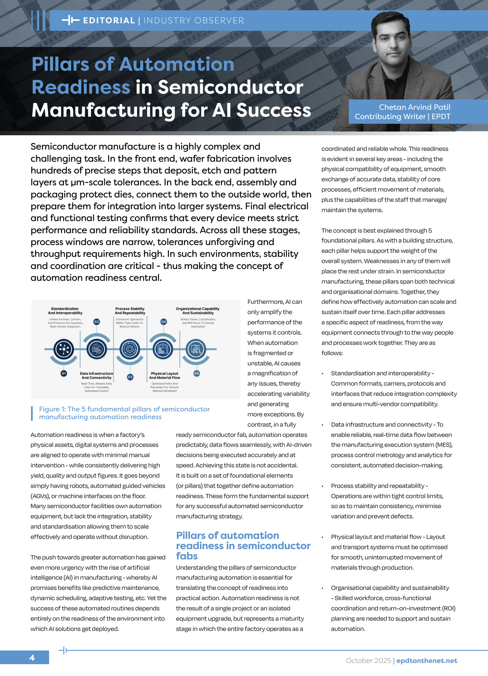
Pillars Of Automation Readiness In Semiconductor Manufacturing For AI Success
Published By: Electronics Product Design And Test
Date: October 2025
Media Type: Online Media Website And Digital Magazine -

The Semiconductor Scaling And The Growing Energy Demand
Image Generated Using DALL·E
The rapid progress of semiconductor technology is built on a simple principle: by scaling transistors down, more components can be packed into a chip, resulting in higher performance.
Over the past half‑century, this strategy has delivered exponential growth in computing power, but it has also unleashed a hidden cost.
As manufacturing processes have become more complex and factories have grown larger, the energy required to produce each wafer and to operate cutting-edge tools has risen significantly.
Let us examine how the pursuit of smaller features and increased functionality influences the energy footprint of semiconductor manufacturing.
Scaling’s Hidden Energy Burden
The paradox of semiconductor scaling is that even as transistors have become more energy-efficient, the total energy required to manufacture chips has continued to rise. In the early 1980s, a survey by SEMATECH and the U.S. Department of Commerce reported that producing a square centimetre of wafer consumed about 3.1 kWh of electricity.
By the mid-1990s, studies published in Elsevier research on fab energy efficiency showed that improvements in equipment and clean-room design reduced this to roughly 1.4 kWh/cm².

Image Credit: EPOCH AI However, this trend reversed in the era of advanced nodes. A recent life-cycle assessment by imec’s Sustainable Semiconductor Technologies program found that cutting-edge processes, such as the A14 node, require multiple patterning and extreme-ultraviolet (EUV) lithography, resulting in energy intensity exceeding 4 kWh/cm². EUV scanners themselves, according to open data on EUV lithography, consume more than 1 megawatt each and use nearly 10 kWh of electricity per wafer pass, over twenty times more than their deep-ultraviolet predecessors.
On the other hand, global energy consumption figures underscore this burden. Azonano’s 2025 industry analysis reported that fabs consumed around 149 billion kWh in 2021, with projections reaching 237 TWh by 2030, levels comparable to the annual electricity demand of a mid-sized nation. The impact of AI is even more dramatic: TechXplore’s reporting noted that AI chip production used 984 GWh in 2024, a 350% increase from the previous year, and could surpass 37,000 GWh by 2030. Meanwhile, SEMI industry reports warn that a single megafab now consumes as much electricity as 50,000 households, while Datacenter Dynamics highlights that TSMC alone accounts for nearly 8% of Taiwan’s electricity use.
In short, scaling has delivered smaller transistors but at the cost of turning modern fabs into some of the largest single consumers of electricity on the planet.
Why Fabs And Tools Consume So Much Power
Building chips at the nanoscale demands extraordinary precision, and that precision comes with enormous energy costs. Modern fabs resemble self-contained cities, running fleets of machines that deposit, etch, inspect, and clean microscopic features while maintaining particle-free environments.
Lithography tools stand out as the biggest energy hogs, but facility systems and even raw material preparation also contribute significantly. The table below highlights how different elements of semiconductor manufacturing stack up in terms of power use and impact.
Taken together, lithography, process equipment, facility systems, and upstream materials explain why fabs are among the most power-intensive industrial facilities in existence.
Each new technology node multiplies the number of steps and tools, pushing power use higher even as individual machines become more efficient.

Image Credit: EPOCH AI
The race to build faster and more capable chips has delivered extraordinary benefits, but it has also exposed the mounting environmental costs of progress. Moore’s law may evolve, but the laws of thermodynamics remain fixed: every advance demands energy.
In all, the path forward lies in pairing innovation with responsibility, thus prioritizing energy-efficient design, renewable power, and sustainable manufacturing. The choices made today will determine whether future chips are not just smaller and faster, but also cleaner, greener, and more responsible.
-

Ins and Outs of The Semiconductor Industry
- Hosted By: MIT Academy of Engineering
- Location: Pune, India (Virtual)
- Date: 25th/26th September 2025