Blog

  • The Semiconductor Foundry Roadmap Race

    The Semiconductor Foundry Roadmap Race

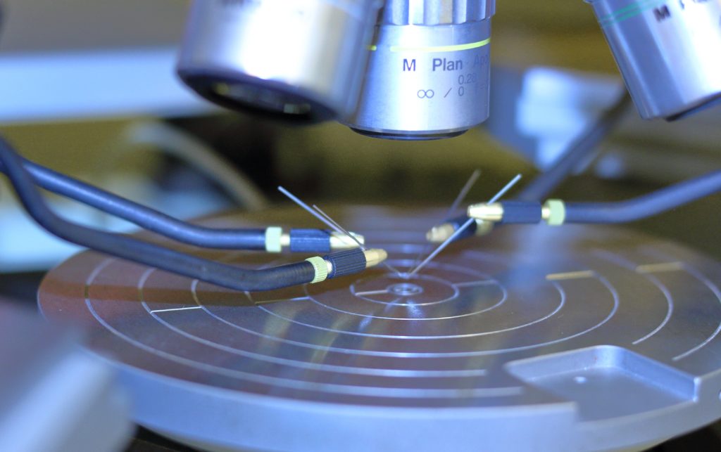
    Photo by Florian Olivo on Unsplash


    THE MAJOR BLOCKS OF THE SEMICONDUCTOR FOUNDRY ROADMAP RACE

    Semiconductor foundries across the globe are focused on providing solutions to retain existing customers and attract new customers. To achieve these two goals, semiconductor foundry companies have to keep innovating. Innovations are critical to ensure the solutions offered by foundries will spearhead the growth of new semiconductor products, thus the customers.

    Semiconductor foundry roadmap plays a vital role in empowering customers with the future of semiconductor foundry technology. These roadmaps require years of research and development and are often in line with where the semiconductor industry is heading. Roadmaps also attract investors, and achieving roadmap milestones without delay is more important than ever. Any slip in achieving the milestones can directly impact customers and can derail market position.

    The semiconductor foundries focus on several aspects of semiconductor technologies to drive semiconductor manufacturing forward. However, there are specific blocks that the majority of the semiconductor manufacturing players focus on as part of their long-term roadmap.

    Technologies: Semiconductor foundries run on different types of semiconductor technologies. These semiconductor technologies are driven based on the product focus and capabilities of a given foundry. Semiconductor foundry fabricating only memory devices is more inclined towards (Example: Micron focuses on novel ways to increase layers of memory cells) providing memory-oriented semiconductor technologies. Similarly, analog, digital, or mixed-signal fabricating foundries focus on next-gen photo masking, etching, passivation, lithography, etc., to set their fabrication technology apart. The drive to focus on a specific technology (as per the foundry requirement) is the primary reason the yearly semiconductor roadmaps (from different companies) are focused on solutions that can enable future semiconductor technologies (devices, materials, etc.). Doing so can also expand the market share.

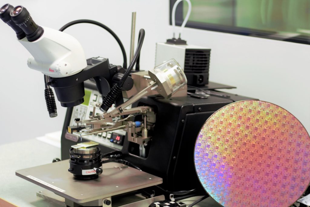
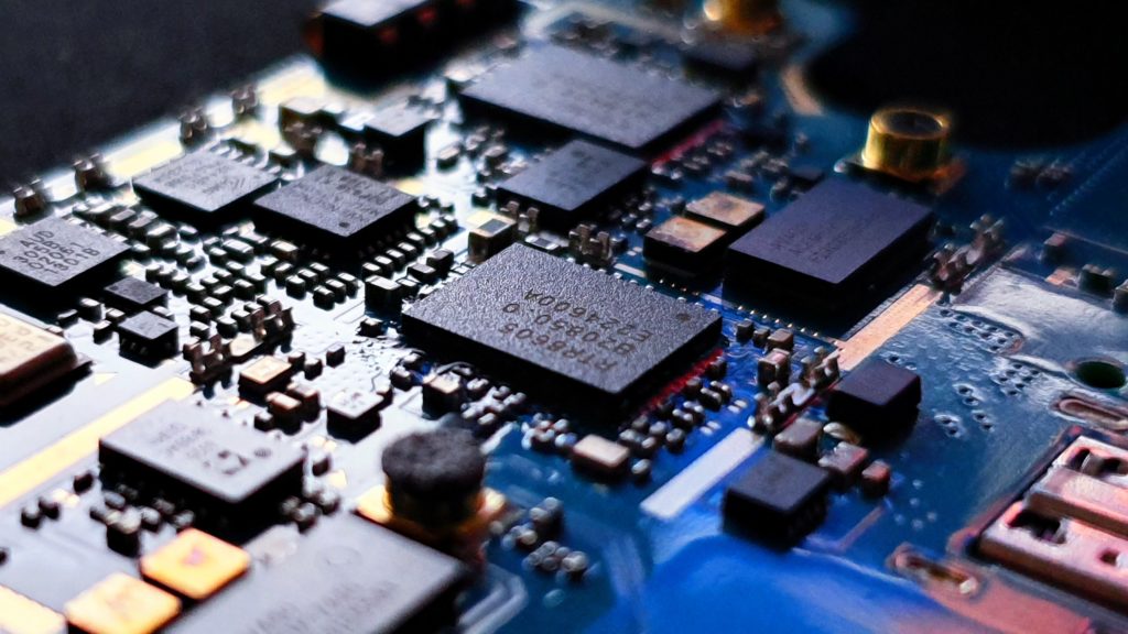
    Devices: Devices are the basic building block of any silicon product. In the last few decades, the size of these devices (FETs) has only shrunk, thus providing more area to pack different types of processing blocks without utilizing a large silicon area. These devices have shrunk in size due to the massive research and development (between academia and industry) activities coupled with advancements in semiconductor equipment technology. Device research and development activities also need to be part of roadmaps to ensure next-gen solutions (like MBCFET, Next-Gen FinFET, etc.) cater to the requirements of both the foundries and the design houses.

    End-Of-Line: Semiconductor fabrication requires three different lines/steps: Front, Middle, and Back. Front-End-Of-Line (FEOL) focuses on creating the structures that make the chip active as per the voltage and current requirements. Back-End-Of-Line (BEOL) process steps are primarily concerned with connecting different layers/blocks via complex interconnects. Lastly, to bridge the gap between the FEOL and BEOL, Middle-End-Of-Line (MEOL) is required. MEOL provides structures that serve as small contacts (like interconnects but have a specific and niche use/purpose during the fabrication) between different active regions of transistors. These three fabrication steps are the base of any silicon product. To keep up with Moore’s law, FEOL, MEOL, and BEOL have to be on the semiconductor foundry roadmaps so that every foundry can differentiate its process technologies from others and in the long term can provide unique solutions.

    Materials: Similar to semiconductor devices, semiconductor materials also are one of the building blocks of semiconductor products. In reality, semiconductor products heavily utilize semiconductor materials during the manufacturing steps. The semiconductor foundry business will not exist without semiconductor materials like Silicon, Germanium, Gallium Arsenide, and several more. Apart from the basic periodic table materials, the semiconductor industry is also dependent on different kinds of chemicals. In the end, the semiconductor industry is built on top of basic science like any other industry is. Almost all semiconductor foundries focus on the materials aspect. However, given the slow change in new techniques around materials, the emphasis on semiconductor materials is not as big as any other aspect of semiconductor fabrication. Continuously improving the device efficiency means that the semiconductor foundries also need to focus on new types (Carbon nanotube, compound semiconductors, etc.) of materials to enable new solutions.

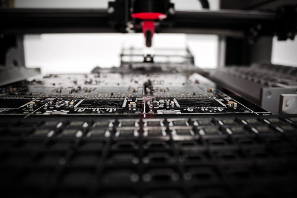
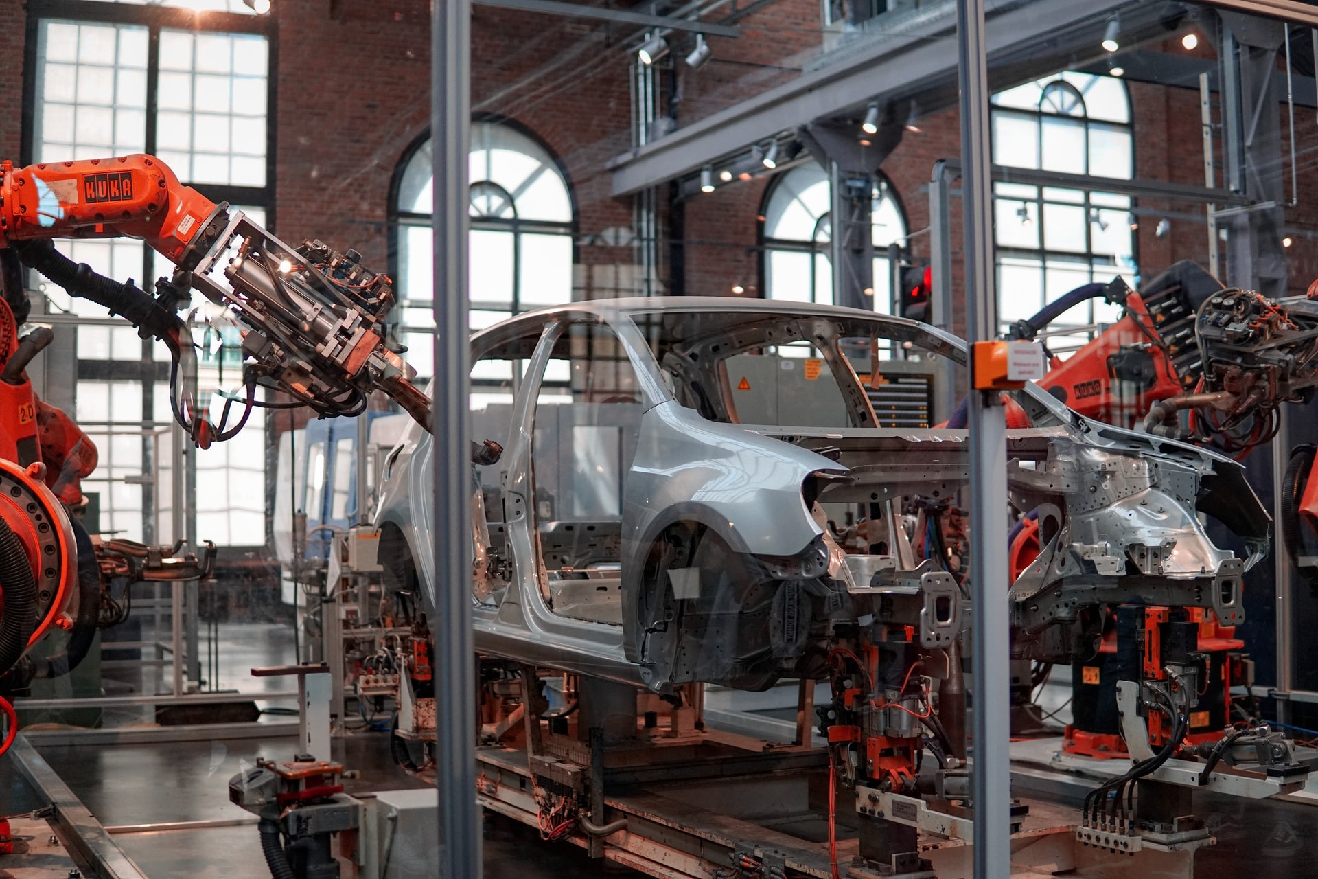
    Automation: Semiconductor manufacturing (fabrication, assembly, and testing) is highly automated and requires minimal human interference to process the wafers. Semiconductor automation plays a vital role in ensuring that the lots get processed with the maximum throughput possible. Along the way, automation also captures/predicts issues that can empower semiconductor foundries with information to avoid delays and cost. The importance of automation has only grown in the semiconductor industry, and the dependency means automation technologies have become the default part of the semiconductor foundry roadmap.

    Semiconductor foundries have focused on roadmaps for decades. It has helped them come up with next-gen technology and has also pushed the semiconductor technology race forward. Semiconductor Pure-Play Foundries and Integrated Device Manufacturers (IDM) are known for charting specific roadmaps that have always driven semiconductor manufacturing forward.

    However, as the race to come up with the next-gen semiconductor manufacturing solutions grows, there is a need to focus on specific solutions that can push the manufacturing aspect of the semiconductor towards the angstrom era of devices.


    Picture By Chetan Arvind Patil

    THE NEW BLOCKS OF THE SEMICONDUCTOR FOUNDRY ROADMAP RACE

    The continuous integration of new devices without increasing the silicon area has provided a new path for semiconductor design and manufacturing. Today, slim and compact electronics products are only possible due to the advent of a new class of semiconductor devices and technology-node that have ensured that the area required is not a hindrance to providing required power and performance.

    Semiconductor researchers in collaboration with foundries have focused on several semiconductor technologies that have pushed the boundaries of semiconductor manufacturing so far. In the years to come, semiconductor foundries will need to focus on the new (examples below) building blocks of a roadmap for the semiconductor foundry.

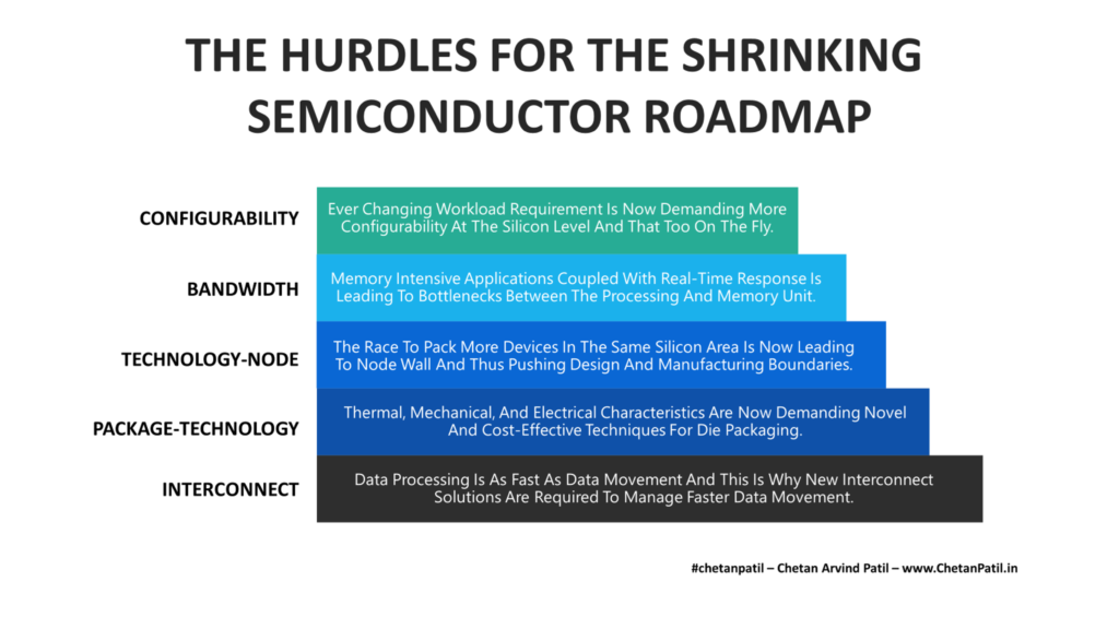
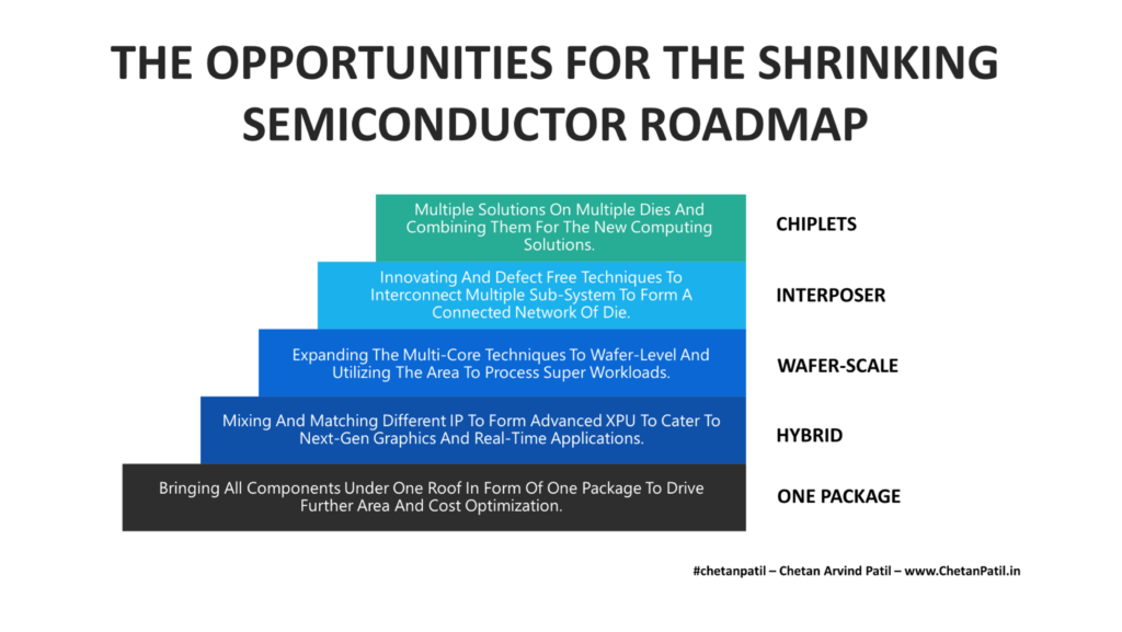
    FIN: The building blocks of semiconductor products are the devices. Until FinFET, these devices were planar. Starting with FinFET, the semiconductor design moved towards 2.5D. However, the need to scale further and put more transistors without compromising power and performance requires using 3D devices built using nanowire (GAAFET) and nanosheets (MBCFET). For increasing transistor density beyond Moore’s era, the semiconductor foundries will have to look into future devices that can utilize the FINs on the FET to drive the industry beyond 1nm and into the Angstrom era. It will require different foundries to focus heavily on a roadmap that purely focuses on developing new multi FIN-based FET devices.

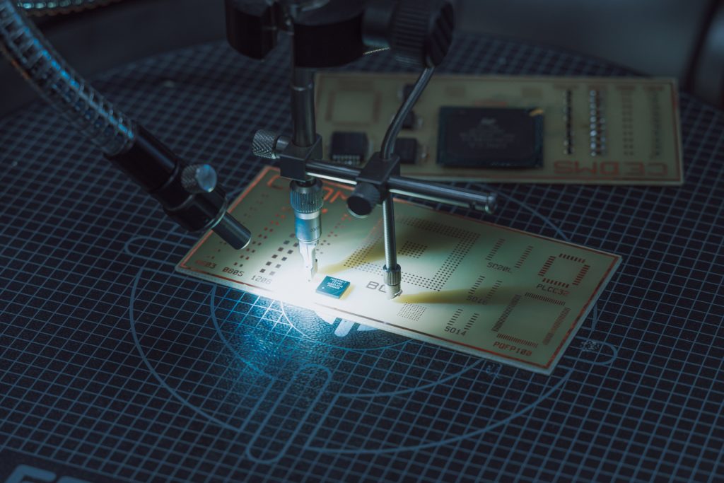
    xUV: Lithography is one of the critical fabrication process steps and also the costliest of all. Today, the most sophisticated UV technology to drive lithography is Extreme Ultraviolet (EUV). Only a handful of semiconductor foundries around the globe are capable of fabricating wafers using EUV equipment. The reason is the cost and also the fundamental issue like defects leading to reliability concerns. Technology like EUV is critical to meet semiconductor foundry’s technology-node goals. The semiconductor industry is on its way to surpass 2nm technology-node, which will require cost-effective and error-free lithography techniques that can enable devices transistors size of 1nm and beyond. It is only possible if semiconductor foundries work with semiconductor equipment manufacturers to drive a roadmap for next-gen lithography technology-powered equipment.

    ABCD: Semiconductor foundries are fabricating hardware devices, but doing so requires several software solutions to keep the production line up and running apart from achieving the high yield, low defect, and faster throughput. All this is possible due to the focus on the ABCD (A = Artificial Intelligence, B = Big Data, C = Cloud, D = Digital Transformation) approach the semiconductor foundries have taken for a long time. As the world moves towards new semiconductor capacity, the need to drive next-gen ABCD solutions that are low on cost but high on efficiency will grow. Semiconductor foundries will have to keep innovating internally to ensure that the ABCD approach gets implemented via a roadmap to achieve the target (yield, scrapping, errors, etc.) results to drive minimal waste with maximum output.

    Stacking: FinFETs tool the semiconductor industry from 2D devices to 2.5D devices. And today, the semiconductor industry is gearing to expand the FINs to enable the next-gen devices like CFET. CFET utilizes the folding approach to keep nFET on top of the pFET, thus securing the stacking approach for a real 3D integration. Stacking will also ensure that the next-gen devices utilize far less silicon area than today’s devices. It also requires innovation on the package-technology side, but the first step is always fabrication. Several device-level solutions exist that can transform horizontal integration into vertical. It will ensure the semiconductor industry keeps increasing the transistor density. However, there are still thermal, electrical, and failure (apart from cost) challenges that require a continuous improvement plan with the help of long term stacking roadmap.

    Efficiency: Semiconductor products are defined based on how efficient they are. Efficiency does not mean low-power consumption but is about achieving the perfect balance of power, performance, and area (PPA) as per the target application. To achieve the balance of PPA, several semiconductor technological solutions from equipment, wafer size, devices, materials have to come together. Devices might be the most dominating aspect of achieving a balanced PPA. However, to fabricate these devices, different other semiconductor building blocks are required. Semiconductor foundries will have to have a roadmap that focuses on the power, performance, voltage, and area characteristics of the next-gen technology-node is at par with any given solution that exists today.

    Several semiconductor manufacturing companies are gearing up to increase the worldwide installed semiconductor manufacturing capacity. However, increasing capacity is only half the job done. What is needed is the focus to keeps bringing new semiconductor manufacturing technologies that can excite the customer and drive the market towards a new era of semiconductor solutions.

    The new upcoming semiconductor foundry capacity will require a semiconductor roadmap that drives new types of technology-node, equipment, automation, and other solutions. Semiconductor foundry’s roadmap from different competitors will ensure tomorrow’s semiconductor products are better than today’s and will also push the innovation around the products that semiconductor silicon devices are powering today and in the future.


  • The Semiconductor Manufacturing Struggles

    The Semiconductor Manufacturing Struggles

    Photo by L N on Unsplash


    THE KNOWN SEMICONDUCTOR MANUFACTURING STRUGGLES

    The cost of semiconductor manufacturing is doubling every four years. The major driving factor for the rising cost is the product complexity due to the introduction of new technology-node and packaging technologies. Electrical testing also has played a role in increased manufacturing costs due to the demand for advanced automated equipment.

    All such costs are directly associated with the increase in transistor density with shrinking die area. The increase in transistor density has also lead to several semiconductor manufacturing struggles. These struggles (have been around for decades) are an indispensable part of the semiconductor manufacturing process.

    Advanced and automated equipment often helps solve the unknown and known struggles. However, the demand to increase the number of lots processed per hour adds a constant pressure to ensure that every wafer/die/product that gets processed is using an error-free recipe.

    While the semiconductor manufacturing process has numerous steps, some steps do require special attention to capture any issues before it leads to shipment of bad products/parts.

    Defect: Fabricating, testing, and assembling thousands of dies often leads to defect. The defectivity rate is considerably low today than it was a few decades back. However, recipes are required to ensure that any wafer or assembled part is defect-free. Capturing defects is a manufacturing struggle, mainly due to the increasing layers/devices in the small silicon area. Sophisticated tools do capture defects, but a new type of defect can escape the fabrication scrutiny. Any such escape leads to known struggles of increase in processing time and cost.

    Quality: Qualifying products is an important pillar of semiconductor product development. Depending on the product type, the qualification process has to follow standard steps before the product can be mass-produced. The industry standards do allow the easy flow of qualification. However, it is still a big struggle to ensure that all checks and processes get implemented correctly. As semiconductor products become more advanced, the cost and time associated with qualification (and failure analysis in case of part failure in the field) processes are rising. All this is pushing the qualification part of the semiconductor product development through the unknown to known struggles.

    Data: Semiconductor and data go hand in hand. For decades, designers and manufacturers have spent a lot of time and effort to streamline a data-driven semiconductor product development process. However, as new advanced products get designed/manufactured, the cost of data capturing, analyzing, and storing is also rising. It is another struggle that the manufacturing process has to deal with. On the positive side, data today has become an integral part of semiconductor manufacturing, and so have been the tools to support data science activities to capture processes to defects. In the long run, the data struggle will keep increasing.

    Break-Even: Cost of fabrication, testing, and assembly is rising. The capacity crunch is adding fuel to it. As new semiconductor technologies get launched, the cost of semiconductor manufacturing is rising. It also means that semiconductor manufacturers have to struggle their way through a long time before they can start earning net positive revenue. While this is true for several other manufacturing industries, the high CapEx that semiconductor manufacturing requires is very high and comes with risks.

    Equipment: Every new semiconductor manufacturing technology (technology-node, package-technology, materials, chemicals, etc.) also pushes the need for a new type of equipment. It puts the FABs and OSATs through a continuous cycle of semiconductor manufacturing up-gradation, and also the equipment manufacturers, who have to struggle their way out to keep bringing new advanced equipment to drive next-gen semiconductor manufacturing technologies.

    The above processes are just the handful of known struggles that any semiconductor product has to go through. Several sub-processes also exist and also require continuous monitoring to identify any known/unknown manufacturing issue.

    Semiconductor manufacturing already has several recipes and equipment to ensure that the target number of lots is processed per hour, apart from ensuring that every wafer/part works as per the specification. However, to achieve such a goal also means to overcome several unknown issues that can show up during the semiconductor manufacturing process.


    Picture By Chetan Arvind Patil

    Picture By Chetan Arvind Patil

    THE UNKNOWN SEMICONDUCTOR MANUFACTURING STRUGGLES

    Apart from the known semiconductor manufacturing struggles, several unknown issues can pop up during semiconductor manufacturing (fabrication, testing, and assembly). These struggles are not like never seen before but remain classified as unknown due to the new information that is generated when such issues occur during the semiconductor manufacturing process.

    Known Struggles: These struggles are part of the product by default, and a set process to capture issues around these processes already exists.

    Unknown Struggles: These struggles are similar to known ones, but often through-off the product flow due to new issues that never existed before.

    The time, cost, and efforts required to solve these unknown mysteries often impact the development cycle time. Any slip or late capturing of unknown issues can further increase the CapEx required to drive the product manufacturing and might put the semiconductor companies in tough spots.

    Yield: Yield can make or break a semiconductor product. The data captured at every manufacturing step has a direct or indirect impact on the total yield. Yield issues, if any, are often based on several factors. While the majority of the yield issues can be solved without extra time/cost, there are often unknown issues that take up a lot of time and effort. As semiconductor manufacturing becomes complex (new devices), there will be unknown yield issues that will keep bringing unknown struggles.

    Throughput: Keeping high uptime is a challenge for FABs and OSATs. However, there are often issues that are not known and can lead to lower throughput, and thus increases the cycle time of semiconductor product development. Throughput struggles are due to equipment downtime, new process testing, high demand, capacity crunch, and several other factors. The last two years have already shown how such unknown (high demand) throughput struggles are affecting the semiconductor supply chain.

    Scheduling: Managing thousands of orders is a big challenge of semiconductor manufacturing. Scheduling techniques are used to ensure all the products/wafers are processed in a timely manner. Any unknown spike in demand or issue with any of the processes brings unknown scheduling challenges for the FABs and OSATs, and they often have to re-prioritize activities to ensure the cycle time does not increase for their customers. This is another unknown struggle semiconductor manufacturing has to often deal with.

    Wafer Size: Every FAB and OSAT is defined based on the wafer size/capacity. There is a point wherein FABs and OSATs realize that the current wafer size/capacity is not enough. It implies FABs and OSATs now have to invest in new facilities, which brings an unknown challenge of whether the semiconductor manufacturing capacity should be based on new wafer size or should only be an expansion of current facilities (with same wafer size). The answers to these simple questions severely impact the future roadmap of any semiconductor manufacturing company and thus brings unknown planning and investment questions/struggles.

    Handling: Materials are constantly moving in the FAB and also in the OSAT. Often the automated system used to drive material handling and processing go down, and several impacts material handling/processing. Such downtime of material handling brings unknown scheduling to processing challenges. It also often happens that the manual handling of materials leads to wafers getting scrapped, and this is another unknown variable that can occur anytime during semiconductor manufacturing.

    Like any manufacturing industry, the semiconductor industry/manufacturing has to go through different phases of known and unknown struggles. These struggles do impact the time or the cost aspect of semiconductor manufacturing and often both.

    In the last four to five decades, semiconductor manufacturing has seen several advances (technology to processes to facilities) that have only helped ease the manufacturing of semiconductor products. As the world moves towards more semiconductor-driven products and solutions, the hope is that new next-gen semiconductor manufacturing solutions (tools, equipment, data-driven approach, etc.) will lower the known and unknown semiconductor manufacturing struggles.


  • The Hurdles And Opportunities For The Shrinking Semiconductor Roadmap

    The Hurdles And Opportunities For The Shrinking Semiconductor Roadmap

    Photo by Matt Duncan on Unsplash


    THE HURDLES FOR THE SHRINKING SEMICONDUCTOR ROADMAP

    Several roadmaps get initiated by different semiconductor companies and also semiconductor technical bodies. These roadmaps provided a path of where semiconductor technologies were, where it is today and where it will be tomorrow. In many cases, roadmaps also allow a way to understand how the product development phase will be for any given domain within the semiconductor industry or company.

    These roadmaps are based on the capabilities of any given company to drive semiconductor technological innovation. These innovations then eventually push the industry towards the next-gen of solutions that set the path for future research and development. For example, the mass production of 2nm is heavily dependent on EUV technology, and when such a solution is used at a large scale then enables the development of more die-to-device-level optimization and research.

    However, the continuous push to innovate and provide more balanced power and performance has now brought the semiconductor industry to a point where there are several challenges that companies (and the industry at large) need to overcome. These challenges will eventually enable new opportunities that will move the semiconductor product innovation ahead.

    Configurability: The computing workloads in the 1990s were far less complex than the workloads today’s computing architectures are running today in the 2020s. For lighter workloads, a rigid IC (mainly XPUs) is perfect. Today, the workloads are changing due to the new data that gets generated faster than ever. That demands configurability from the lower level architecture to drive away any architectural bottlenecks. Configurability at the silicon level is all about adapting internal features based on the workload type. Configurability is hard to validate (apart from making it hack-proof), and the mass production of high-level configurable architecture remains a distant dream and a big challenge.

    Bandwidth: Memory-intensive applications often require XPUs to read and write data to/from memory at a fast speed and that too at a high rate. Such continuous data movement is possible only if the memory bandwidth is large enough to drive faster data throughput. Theoretical maximum memory bandwidth overall has been increasing. It is mainly due to new XPUs that utilize memory interfaces via a high-bandwidth memory controller. There are applications (on the server-side) that require much larger bandwidth for faster GB/second to keep up with the read/write request from the processing unit. It is a challenge for semiconductor memory companies, as they gear up for the 5G+ and Edge computing world where every data point will have to get processed on the go.

    Technology-Node: Research-driven design and development have enabled the shrinking of transistors. Today billions of transistors get fabricated in silicon chips to provide the highest performance possible. However, the race to pack more devices is now leading to a device scaling bottleneck. On top of that, device scaling is also pushing the boundaries of science (physics, chemistry, and math). The semiconductor industry is still marching ahead and is ready to touch the 1nm technology-node and then move to the angstrom era. The design and manufacturing challenges brought with the new device scaling era will be endless. The semiconductor industry will have to move beyond just focusing on the shrinking of the technology-node.

    Package-Technology: The shrinking transistor size is not only affecting semiconductor manufacturing but also has impacted package-technology. The semiconductor industry has already found solutions by utilizing 2.5D/3D techniques as an avenue to drive next-gen package-technology. There are still thermal, mechanical, and electrical challenges that are not easy to solve with every growing silicon density. Today, disintegrated packaging solutions are being used to integrated different components to balance the device characteristics.

    Interconnect: Any given silicon product has different blocks interconnected via different network topologies. Interconnect allows data movement and transfer between multiple processing units. The speed of the processing units itself drives the application response time. As the number of processing units has increased in XPU, managing the data traffic is becoming a challenge. The electrical interconnect is also leading to higher power consumption as the data traffic is increasing. Thus putting the semiconductor solutions to adopt for alternate techniques to drive next-gen interconnect. Optimizing other alternate interconnect (photonics) solutions is going to be a big challenge for XPU designers.

    The semiconductor industry has followed the roadmap approach for a very long time. Such a continuous outlook has pushed the boundaries of semiconductor design and manufacturing. The roadmap is also the reason why several innovative semiconductor-powered solutions are coming out in the market. There are certainly challenges due to Moore’s law scaling down. However, these challenges are creating new opportunities and driving the semiconductor industry towards the More-Than-Moore era.


    Picture By Chetan Arvind Patil

    Picture By Chetan Arvind Patil

    THE OPPORTUNITIES FOR THE SHRINKING SEMICONDUCTOR ROADMAP

    The shrinking semiconductor challenges are also an opportunity for the semiconductor industry. These opportunities push the envelope of the semiconductor industry and thus create the roadmap for future technologies.

    The growing need to pack more transistors using different processes or methods has provided the semiconductor industry to drive new design ideas. Several semiconductor design innovations have matured from the research stage and are being used to manufacture next-gen devices. The drive to provide a new optimized approach is opening up the future roadmap for the semiconductor industry.

    These roadmaps are build by the opportunities created by the challenges that the industry faces today.

    Chiplets: Increase in transistor density without increasing the silicon area leads to bottlenecks. These bottlenecks are not only around design (power and performance) but also on the manufacturing side. The manufacturing technologies (via technology-node and equipment support) have advanced to enable device fabrication at 2nm. The thermal, mechanical, and electrical characteristics (due to the small silicon area) are posing a challenge to the XPU design. Such challenges are also presenting a new opportunity for XPU designers. Semiconductor XPU design companies have now adopted the multi-die technique to spread the silicon area, which also has the potential to improve overall yield. AMD and Intel have already demonstrated XPUs with chiplets for multi-die XPUs, and will certainly dominate the market (in terms of design/innovation). 

    Interposer: Chiplets manufacturing required the use of multiple dies. Connecting these different blocks to form an integrated chip/system often requires a specific silicon technology called interposer. Semiconductor companies often use different interposer terminology, but eventually, the underlying goal of each of these is to provide a common place for two or more die/blocks. Interposers usage will grow with the growth in chiplets adoptions. It also means providing optimized network-based topology to arrange/stack different blocks for efficiency, which is an opportunity for the research and development teams across academia and industry.

    Wafer-Scale: Servers to supercomputers are getting faster every year. The need to shrink the data centers while not compromising on the throughput is pushing semiconductor design and manufacturing towards large-scale wafer-level solutions. For such solutions, the wafer-scale integration approach comes in as an opportunity to provide die areas as large as the wafer to create high-performance processing units. These units can then cater to any data demand of today and the future. Due to the advancement in semiconductor manufacturing, the yield at the wafer level will not be an issue, but the cost aspect can be.

    Hybrid: Monolithic chips have been in use for several decades. Later, monolithic chips got replaced by multi-core homogeneous and heterogeneous architectures. As the world moves towards a more remote-enabled world, the need for multiple hybrid architectures will grow. These hybrid architectures will have unique processing characteristics, which will enable semiconductor design and manufacturing companies to leverage new methodologies like chiplets to heterogeneous architectures to mixing/matching IPs, thus providing an opportunity to expand the semiconductor roadmap.

    One Package: System-In-A-Package (SiP) allows a way to integrate multiple systems under the same package technology (carrier package). Given the proliferation of multi-die integration, SiP will take the central stage. One package approach will allow semiconductor companies to provide a unified packaging approach to stick together different dies/IPs under the same substrate. While this will pose a challenge, the past success around similar package technology will smoothen this approach.

    Continuous technology development is the key to ensuring that the semiconductor roadmap keeps moving forward. These new technological solutions also enable different industries that leverage the new design to manufacturing methodology to drive better customer experience.

    As the semiconductor roadmap inches towards the 1nm era, it will be vital to keep innovating to move the world into the angstrom arena.


  • The Requirements And Challenges Of Semiconductor Product Development

    The Requirements And Challenges Of Semiconductor Product Development

    Photo by Brian Kostiuk on Unsplash


    THE REQUIREMENTS OF NEW SEMICONDUCTOR PRODUCT DEVELOPMENT

    The semiconductor industry is driving on top of the products that different companies introduce. These semiconductor products have to go through complex product development procedures to fulfill strict technical and business requirements. That makes the planning and strategy aspect of development vital.

    Technology (devices and package side) progress in the semiconductor industry has powered designers and manufacturers with resources to develop highly complex semiconductor products. These technological advancements have enabled much smaller and portable semiconductor-powered products than ever before.

    More options and features on semiconductor design and manufacturing are a bonus for both companies and their customers. However, the wide range of the device to transistor-level characteristics also means that the requirements to drive new semiconductor product development are getting stricter and thus leaves no room for error.

    Time: Semiconductor products have to go through a different process and validation steps, and this makes the planning of the design and the manufacturing phase a crucial step. Any slip or delay can give competitors an advantage. On top of that, the fast rate at which the different and new semiconductor-powered solutions (smartphones to automotive) are getting launched also puts pressure to ensure that any new semiconductor products are developed at the right time to meet the market/customer requirements.

    Cost: The cost of semiconductor manufacturing is increasing, mainly due to the progress in technology nodes, package technology, and also new automated equipment. Thus, selecting the right combination of semiconductor technology is a crucial step, as it directly affects the cost of manufacturing.

    Area: The shrinking device size (and also new vertical package technologies) means new semiconductor products can power new features in a small chip area. However, doing so demands a mechanism to ensure no design or manufacturing rules get violated. On top of this, the smaller size also means less space to provide more new advanced features. As the technology-node and package technology have made progress, the semiconductor products are also getting designed with the smallest footprints possible.

    Performance: The world is moving at a faster rate than ever. The wireless connected solutions to high-speed computers are all demanding fast processing. Enabling the high-performance (faster decision-making) feature in semiconductor solutions is a vital requirement. While not all silicon products get designed for faster processing, there are several application areas where a quick decision (airbag deployment)) is still the most basic requirement.

    Power: Apart from performance and area, managing power consumption is another de-facto criteria for several semiconductor products. The requirement of power management varies based on the application of the semiconductor product. In the long run, it becomes a very challenging task to managing power without having the room to provide an area for thermal management.

    Balancing all of the above requirements of a new semiconductor product is not an easy task. It requires resources to drive the vision of developing a semiconductor product that can take over the market. That is why today, there are companies (mainly in the XPU segment) that are taking new paths (chiplets, heterogeneous, wafer-scale engine, etc.) to develop new semiconductor products for their end customers.

    As the barrier of entry in the semiconductor industry (from the design point of view – FAB-LESS) has lowered, the competition of developing products loaded with new features has grown too. This has put a lot of pressure on companies to design new techniques that can provide critical features (response time, battery life, heating, etc.) to make their products stand out in the market.


    Picture By Chetan Arvind Patil

    Picture By Chetan Arvind Patil

    THE CHALLENGES OF NEW SEMICONDUCTOR PRODUCT DEVELOPMENT

    The majority of semiconductor products are designed and manufactured by considering the cost and time requirement. These two vital requirements also bring new challenges to the design and the manufacturing houses.

    Ensuring the products meet all the customer requirements has made the development of new semiconductors a challenging process. These challenges are faced by every semiconductor product, irrespective of the company developing it.

    Features: The number of FAB-LESS companies in the semiconductor industry has grown over the last few decades, and has increased the level of competition in the semiconductor new product market. It also means that every other product is equipped with new innovative features like new manufacturing methodology (chiplets) to utilizing new-age devices (MBCFET). The urge to provide new features to differentiate semiconductor products in the market is a challenging task, and it will keep getting more challenging due to the push towards newer semiconductor devices and also manufacturing processes (nodes).

    Validation: Ensuring the new product meets all the requirements and specification is vital. Thus depending upon the application area, the validation standards change too. The longer the validation process takes, the higher the cost associated with it and makes the semiconductor post-silicon efforts in a complex activity wherein both time and cost are to be managed.

    Customer: In the end, semiconductor products will be used by different customers. Understanding and catering to the different customers (and their market) is an important building block of a successful product. The most crucial challenge is to ensure that the product can be developed in the shortest timeline while also providing the rich set of features that the market is pushing semiconductor companies to provide.

    Reliability: New reliability standards are getting proposed to drive higher quality. The major reason for doing so is to meet the new requirements due to ever-advancing silicon/transistor level solutions that require detailed reliability checks to ensure the product does not fail in the field. While this brings cost and time challenges, the efforts required to enable new processes are an added challenge.

    Life: New features coupled with changing market demand are shortening the life of semiconductor products. The short market life of semiconductor products means continuous new product launches. This is the primary reason why every year there is a new generation of XPUs that are being launched with new design and manufacturing solutions. The growing market and competition will further drive down the semiconductor product life from decades to years.

    The standards and set process used by the semiconductor industry allow them to overcome the majority of the above challenges. The high-end equipment to design rules to process recipes has already empowered semiconductor houses to develop the first time right semiconductor product. The future challenges are more towards balancing the advancing technology with the cost, resources, and time in hand. Companies that will not be able to balance all these will face tough competition in the semiconductor market.

    In the next few upcoming years, several new (5G/6G, electric cars, etc.) opportunities will come up for the semiconductor industry. All new challenges will drive the semiconductor industry toward new semiconductor product solutions that cater to different requirements while ensuring the product meets the customer’s expectations.


  • The Automated World Of Semiconductor Manufacturing

    The Automated World Of Semiconductor Manufacturing

    Photo by L N on Unsplash


    THE REASONS FOR SEMICONDUCTOR MANUFACTURING AUTOMATION

    Automation is part of all advanced manufacturing industries. As the computing world has progressed, the high-tech software-hardware interaction now allows manufacturers all over the world to make the most of automation techniques to accurately run their production line.

    Semiconductor manufacturing is one such industry, which has taken advantage of automation for a long time and during this course has deployed several automated techniques to minimize errors. Given the time, cost, and resources required to manufacture semiconductor products, it is inevitable that automation is required to develop semiconductors.

    There are several ways in which automation is deployed to manufacture error-free semiconductor products. This ranges from utilizing software to keep track of different production activities to highly advance equipment that finishes the task with a click of a button. All these automated processes have taken a very long time to perfect and semiconductor manufacturing on itself has also invented many techniques to ensure there are no gaps in their manufacturing process.

    Apart from utilizing automation to ensure that the semiconductor production line is up and running 24×7, there are several other key factors that drive the need for automation in the semiconductor industry.

    Defect: The semiconductor fabrication process goes through several process steps, and with shrinking transistor size, the complexity to fabricate advanced products is increasing. Automation plays a critical role in the fabrication of defect-free products. Defect-free production demands utilizing advanced equipment which can capture optical images to alert the engineering team about unexpected features. Software (loaded with different algorithms) and hardware (equipment loaded with high-end image sensors) are keys to driving defect-free wafer fabrication. The same applies to testing and assembly.

    Data: Semiconductor data is crucial in ensuring that the product is meeting its required specifications. Capturing semiconductor data is half the job done. Post-processing and analysis are vital steps, which demand utilizing either automated data analysis solutions or tools that engineers can use to efficiently screen the data. In the end, data analysis is automation (capturing, storing, visualizing, etc.) driven and can efficiently allow the elimination of bad parts from the production line.

    Testing: Testing of semiconductor products can take place at several key stages. All these stages often require different types of equipment to test and collect the semiconductor data. Such activities are automated so that the equipment can interact with the silicon wafers or assembled products without human interference. This is one of the major reasons why automated test equipment has become a critical part of post-silicon activities.

    Variation: Analyzing optical data of every semiconductor data is crucial. High-speed devices are utilized to capture images that can find anomalies with the fabricated product. There are also dedicated automated tools that can look inside the devices to find any variation in the fabrication process that can cause the product to fail. Capturing such or any other process-related information and analyzing it in the shortest time possible is crucial in ensuring the end product meets the customer requirements.

    Throughput: Ultimately, the goal of semiconductor manufacturing is to ensure that the semiconductor production line is 100% occupied day in and day out. That is only possible if there are tools, equipment, and data processing systems that can take decisions without delay, which requires investing in equipment apart from the software solutions that enable high throughput. As the back-end activities (fabricating, testing, or assembling) are becoming costlier, fully utilizing semiconductor manufacturing capacity is the need of the hour, which eventually drives the revenue.

    As the world moves towards newer semiconductor manufacturing capacity, the need for automation will only grow, which presents a unique opportunity for both the software and equipment vendors to deploy new solutions.

    The automation market for semiconductor manufacturing will keep growing along with the growth in the semiconductor market and the need for new semiconductor fabrication, testing, and assembling facilities. In the next few years, several semiconductor manufacturing houses are also going to upgrade their facilities. All these presents new opportunities to drive automation within the semiconductor manufacturing industry.


    Picture By Chetan Arvind Patil

    Picture By Chetan Arvind Patil

    THE ROADMAP OF NEXT-GEN SEMICONDUCTOR MANUFACTURING AUTOMATION

    Semiconductor manufacturing utilizes the most advanced manufacturing processes in the world. The technology required to drive these processes needs to be automated and flawless and is the primary reason why semiconductor manufacturing has embraced automation since its inception.

    Over the last few decades, these basic to advanced automated (handling material, moving material, fabricating, testing and assembly, etc.) have seen a lot of improvements and have played a key role in minimizing the Defective Parts Per Million (DPPM).

    The increasing share of the semiconductor market (mainly in critical areas like aerospace, automotive, wireless communication, etc.) will increase the rate of semiconductor fabrication, testing, and assembly. This is the primary reason why the semiconductor industry’s new benchmark for defectivity rate is Defective Parts Per Billion (DPPB), to ensure that the manufacturing process leads to a minimum to zero waste.

    Achieving such a goal is not an easy task and requires bringing different solutions to drive next-gen semiconductor manufacturing automation. There are several advanced techniques that can be deployed to ensure the DPPB is lower than ever, and utilizing automation is key, but it also demands a new approach towards semiconductor manufacturing automation.

    Adoption: As the newer devices and semiconductor processes get deployed, semiconductor manufacturing houses will have to adopt new techniques that can adopt a new data-driven approach to drive the development of next-gen devices. It can be from learning the behavior of the device at every process step to how the testing/validation phase affects the semiconductor product based on the fabrication technology and assembly process used.

    Inspection: As the semiconductor world moves towards 2nm technology-node and beyond, the importance of visually analyzing the devices during every stage of the manufacturing process will be crucial. Doing so requires a highly sophisticated and high-speed instrument that can capture the internal details on the go apart from simultaneously processing the information in a user-friendly manner. While such techniques are already available in the majority of the high-end semiconductor manufacturing facilities, the need to handle a new type of device will mean upgrading the majority of the equipment and software solutions to meet next-gen requirements.

    Equipment: Semiconductor manufacturing equipment is already highly automated and can perform tasks with minimal human interference. However, all the equipment still requires human support (issues with the process steps to fabrication mistakes) apart from regular maintenance. Shortly semiconductor equipment (lithography to etch) will need to get equipped with features that can capture deviation in the process step and thus alerting the production line before more bad parts get fabricated in the subsequent process.

    Comparison: Data capturing and analysis are already part of semiconductor manufacturing. The critical step the semiconductor manufacturing process needs to march towards is a faster and accurate comparison of new, old and relevant data. It can ensure that the semiconductor product getting fabricated does not have any characteristics that were in any other product/data that caused failure in the field. Such techniques can take the automated analysis in semiconductor manufacturing to the next level and thus can lower the failure rate.

    Human: Semiconductor manufacturing is already highly advanced, and as more new facilities come up around the globe, new automated techniques will get deployed. It can range from analytics tools to data-driven equipment. In the end, whichever way the semiconductor manufacturing automation goes, the talent (human resource) required to drive these solutions will be the key. To enable a new level of automation, semiconductor manufacturing will require highly trained human resources that can utilize advanced solutions to drive the automated world of semiconductor manufacturing.

    In the next five years, the worldwide semiconductor manufacturing capacity will increase by 10-20%. All these new (and upgrading older facilities) will require techniques to achieve the lower defectivity and failure rate. It will be possible with the help of automation techniques that can remove the error before they appear. These solutions are already present but will have to get adopted for future devices, technology-node, and assembly processes.

    The semiconductor manufacturing automation presents a new opportunity to both established and emerging companies providing automation solutions, and all these new solutions will improve the throughput of worldwide installed capacity.


  • The Blocks Of Semiconductor Supply Chain

    The Blocks Of Semiconductor Supply Chain

    Photo by Barrett Ward on Unsplash


    THE BUILDING BLOCKS OF SEMICONDUCTOR SUPPLY CHAIN

    Supply Chain Management (SCM) is part of every manufacturing industry. It enables the movement and management of finished goods and all those components that drive the development of the final product.

    As the world became more connected, real-time information allowed SCM to be more efficient than ever. However, the years 2020 and 2021 have brought massive challenges to the SCM. Irrespective of the manufacturing industry, SCM teams across different companies have to fight against the unpredictable trend of the market, and companies (and SCM teams) are now struggling to find avenues to tackle the fluctuating supply and demand in the market. The same challenges and stories also apply to the semiconductor industry. The long manufacturing cycle time has thrown all SCM methodologies and rules out of the window.

    Like other industries, the semiconductor supply chain is also dependent on many blocks. Thus, the semiconductor supply chain also needs a synchronized approach to make materials and resources available so that semiconductor manufacturing can fulfill customer demand without delay.

    To achieve this goal, some of the basic building blocks of the semiconductor supply chain need to work in synchronization. Any delay or bottleneck in any of these basic blocks severely impacts the end customer.

    Raw Materials: The manufacturing of semiconductor products is dependent on the availability of raw materials like chemicals, semiconducting materials (silicon, germanium, gallium arsenide, etc.), substrate, and many other different types of resources. Without procuring these basic materials, the semiconductor product supply chain will not move forward. The semiconductor shortage is not only because of the capacity constraints but is also due to the impact pandemic had on raw material providers. As long as the industry providing raw materials to the semiconductor industry does not face supply chain challenges, the semiconductor supply chain keeps moving forward. If not, then the impact on these critical blocks often leads to a long semiconductor manufacturing cycle time.

    Design: Raw materials are critical from the manufacturing point of view. But before a semiconductor product goes for manufacturing, the design stage needs to be completed. Delays in product design also affect the manufacturing plan and thus directly impact the supply chain. The semiconductor supply chain keeps moving forward with the help of older products. However, the changing landscape and the rush to introduce new solutions means that new semiconductor products should continuously feed into semiconductor manufacturing to keep the semiconductor supply chain active. All this makes semiconductor product design the most vital building block of the semiconductor supply chain.

    Manufacturing: Semiconductor manufacturing is another vital process that semiconductor supply chain management runs on. In reality, this is true for any manufacturing industry, not just semiconductors. The pressure on the semiconductor supply chain today is majorly due to the bottleneck in semiconductor manufacturing. All-time high lead time is stopping the supply chain from providing the customers with the required product in the proper time frame. Supply chain teams often rely on inventory to tackle such scenarios, but the cycle time and lack of pre-planning have taken this option away from several companies. On top of all this, new semiconductor products are getting introduced continuously and entering the manufacturing cycle, which is also not helping semiconductor supply chain management. All this clearly shows why manufacturing is another building block of the semiconductor supply chain.

    Logistics: The movement of goods (whether raw or finished) is one of the most critical processes to drive a flawless semiconductor supply chain. Semiconductor companies worldwide rely on major logistics players to ensure that different parts, products, and materials get delivered on time. Logistics delays also have a direct impact on the supply chain. Thus far, during the capacity constraint, the semiconductor industry has managed the logistics very well compared to a few of the other building blocks of the semiconductor supply chain.

    Inventory: Keeping products in hand for future demand is the base concept of efficient supply chain management. Semiconductor companies often hold either assembled products or fabricated wafers for future requirements. However, this means predicting the future demand without knowing what will and what will not work. Thus making inventory management is another building block of the semiconductor supply chain.

    It is vital to understand why the last two years have been challenging for the semiconductor supply chain. Maybe the answer lies in the methodologies, approaches, and tools that enable the semiconductor supply chain. It might be that older techniques did not work as planned. This course correction is required.

    Given the vast amount of data and on-the-go information, the semiconductor supply chain should have adopted future trends faster and accurately. However, it seems like, in reality, the techniques are not getting utilized along with the resources, solutions, and tools that are available. It is time to revisit few blocks of the semiconductor supply chain and adapt these to create future building blocks that can contain the future semiconductor shortages.


    Picture By Chetan Arvind Patil

    Picture By Chetan Arvind Patil

    THE FUTURE BLOCKS OF SEMICONDUCTOR SUPPLY CHAIN

    In the 1960s, the SCM followed a fragmented methodology and thus required coordinating with different teams to merge the information (forecast, sourcing, logistic, etc.) before implementing decisions. By the 1990s, the fragmented approach became consolidated, and SCM became more centralized. Now, teams could take decisions faster than ever. However, in the 2020s, when the world is more connected than ever, all the information in hand could not predict the market trend. The impact of all this is capacity to supply chain constraint. Today is the time to understand the bottlenecks and prepare future semiconductor supply chain countermeasures that can take into account the abrupt cycle nature of the market.

    To tackle future semiconductor supply chain challenges, the following critical blocks should be re-visited to capture the improvements required along with the way these resources are utilized to make future projections.

    Data: Understanding the market demand is very important. Semiconductor supply chain teams have resources that can allow them to gauge the market swing. These resources provide information to make a better decision on how to manage inventory, manufacturing orders, and supply. However, looking at the pandemic scenario, the semiconductor teams focused on the supply chain have not taken full advantage of the resources in hand. The future decision should be based on new advanced tools that can provide information outside of the industry (like predicting pandemics) and/or developing dedicated talents capable of using data to predict future market changes that can severely affect the semiconductor supply chain. Supply chain management should move more towards data drive management.

    Adoption: Just In Time (JIT) is a widely used methodology in manufacturing. However, the semiconductor supply chain needs to move beyond the traditional concepts. This demands changes in the supply chain working with the help of a detailed understanding of both technical and non-technical (like weather, outbreak, etc.) information that can affect the semiconductor supply chain.

    Planning: Semiconductor supply chain planning should utilize more data points than simply relying on forecast or market intelligence. The roadmap to manage the supply of semiconductor products in the market should also consider data points from different forward and backward supply chain-dependent industries. This could be from understanding the raw material supply chain to the end customer supply chain. Merging several output supply chains can provide a better outlook as to whether the planning is in line with the market reality or not.

    Priority: In the end, decisions taken by the semiconductor supply chain teams are all about how to balance and prioritize product manufacturing. This also means some products will have more supply than others, and any incorrect priority decision will lead to supply constraints. Prioritizing products is not an easy task, and that is why semiconductor supply chain teams need to find new ways to balance the inventory of different types of products.

    Risk: Eventually, semiconductor supply chain management is a risky business. If the market demand is lower than the expected supply (which means the products are at the manufacturing stage), then it can lead to losses. On another side, if the product supply is not meeting the market demand, then the opportunity to gain on the high demand is lost. It is vital to take risks but based on new strategies and concepts that are more robust than the older production and supply systems.

    The semiconductor supply chain teams can take these blocks and re-invent them to their potential. In the long run, the end customer also needs to backtrace and understand how the semiconductor supply chain drives them and also affects them.

    As the semiconductor world moves forward, the semiconductor supply chain management across different industries (not just semiconductors) will also evolve, and supply management teams will have to capture the impact of worldwide supply chains (semiconductors impacting automotive) and how individual industries should master 360-Degree views for long-term benefits.


  • The Semiconductor Manufacturing Cluster

    The Semiconductor Manufacturing Cluster

    Photo by Louis Reed on Unsplash


    THE REASONS TO DEVELOP SEMICONDUCTOR MANUFACTURING CLUSTER

    Developing a dedicated semiconductor manufacturing infrastructure from scratch is a billion-dollar risk and the cost of doing so is also increasing year on year. As the semiconductor industry marches towards a new era of capacity creation, it is important to invest in strategies that can enable a high return on investment.

    Today, the majority of the big semiconductor manufacturing companies are looking for new regions to create their next-gen semiconductor device fabrication, assembly, and testing infrastructure. The cost of making the wrong choice for such a large investment is very high.

    The time, and effort required to build semiconductor manufacturing infrastructure are pushing companies, and also governments, towards utilizing (or creating) regions that already have a semiconductor history. This is one of the major reasons why companies like TSMC, Intel, and Samsung are focusing on regions that already have a large presence of semiconductor companies (end-to-end), as it allows them to make the most of the existing ecosystem and thus drives their new facilities towards breakeven.

    Semiconductor Manufacturing Cluster: A dedicated region or area, where within proximity different semiconductor companies have facilities to provide semiconductor device fabrication, assembly, testing, and distribution services. This area may and may not house a different number of semiconductor design companies.

    When multiple semiconductor manufacturing companies are located in the same region, then a semiconductor manufacturing cluster is formed. A semiconductor manufacturing cluster provides several benefits. These benefits are more geared towards semiconductor companies but in the end also benefit the city or the region where these clusters are located.

    Collaboration: A region with multiple semiconductor manufacturing (and design) companies enables collaboration that can drive the development of next-gen solutions and thus benefits the semiconductor industry at large.

    Optimization: Semiconductor manufacturing cluster will allows the development of several business resources that can aid companies. This can range from raw materials to near-by equipment provider to several other support systems that semiconductor manufacturing companies often need.

    Research And Development: The proximity of advanced semiconductor manufacturing facilities allows companies to develop research and development infrastructure. This is often in collaboration with the government and universities. Doing so speeds up development of new devices that can provide much better efficiency and thus pushes the development of new semiconductor-driven products.

    Ecosystem: Worldwide, there are different semiconductor manufacturing clusters. Some are in Taiwan, some in China, and many in the USA. All these regions have transformed themselves into powerhouses and are now an ecosystem for emerging semiconductor manufacturing facilities.

    Talent: In the end, human resources are vital for any industry. The same applies to the semiconductor manufacturing facilities wherein different skills are required to drive the development of semiconductor products. Semiconductor manufacturing cluster creates an infrastructure that attracts talents from all over the world.

    Semiconductor manufacturing clusters are not built overnight. It takes years of effort from both the government and private players. In many cases, a single entity starts from scratch and there on goes on attracting future companies. There on, over an extended period creates the semiconductor manufacturing cluster on its own. Also, having a university with a very high research and development focus is also an important factor in driving cluster-based semiconductor manufacturing regions.

    Worldwide, as governments attract new investments towards semiconductor manufacturing, it is worth planning by focusing on strategies that can eventually turn the regions into a semiconductor manufacturing cluster.


    Picture By Chetan Arvind Patil

    Picture By Chetan Arvind Patil

    THE STEPS TO BUILDING SEMICONDUCTOR MANUFACTURING CLUSTER

    Developing a dedicated semiconductor manufacturing cluster is not an easy task. It takes years of planning, investment, collaboration, failure, and risk to create one. This is the primary reason as to why there are only a handful of countries that have semiconductor manufacturing clusters.

    Semiconductor clusters can be classified into two types:

    Multiple Companies Multiple Facilities (MCMF): A specific region where multiple semiconductor manufacturing companies come together to create their own separate semiconductor manufacturing infrastructure to drive device fabrication, assembly, and testing.

    Multiple Companies Single Facility (MCSF): A specific area or a region where multiple semiconductor manufacturing companies invest to create a single large facility to provide fabrication, assembly, and testing services for different semiconductor companies.

    MCMF is very common and countries like Taiwan, Japan, South Korea, China, and the USA already have several such regions which cater to different needs of semiconductor manufacturing.

    On another hand, MCSF is very rare and the major reason is the effort required to bring different stakeholders to invest in a single facility that can cater to the manufacturing requirements of different semiconductor players. Today, planning for MCSF might be more favorable due to the cost and time, but there have been several examples where such collaborative strategies have failed.

    Countries looking to develop a region that purely focuses on semiconductor manufacturing need to plan for the next century and not a decade, and the following steps can provide a roadmap of achieving the goal of developing a semiconductor manufacturing cluster, which is what countries without semiconductor manufacturing history need today.

    Government Support: Government support is crucial in driving the development of policies, incentives, and facilities that can cater to the semiconductor manufacturing cluster. This is why countries looking to attract new semiconductor manufacturing investment should develop strategies to make an investment from private players a long-term collaboration.

    Private Partnerships: Semiconductor manufacturing clusters today will require move JV between different semiconductor companies. While single entities can themselves invest in new FABs and OSATs, but in the long run, the region needs to develop by continuously attracting new investment. This is possible if in the initial phases more JVs are formed to drive the development of the semiconductor manufacturing cluster that future private players can take advantage of.

    Aligned Goals: Both government and private players need to be on the same page so that the region chosen as a dedicated place to develop the next-gen cluster thrives for several decades. This requires not only planning for the semiconductor industry but also building regional facilities like logistics to universities and several other plans to drive day-to-day facilities. 

    Future Roadmap: In the end, dedicated clusters are divided into sub-regions that are owned and operated by different entities. However, if there is no future roadmap as to why several companies are bringing new investment (mainly if the cluster type is MCSF) then the future roadmap may not be beneficial. Hence, companies need to collaborate more to drive new manufacturing methodologies.

    Continuous Investment: Semiconductor manufacturing clusters are difficult to build and to make the most of it, continuous investment is required. This can be in the form of new investment policies from governments to attract new semiconductor companies to build new facilities (example: TSMC in Arizona) that can take the region towards a new era.

    There are multiple ways of attracting new investment into new regions/countries. Semiconductor manufacturing cluster vision and planning is one of doing so. This way, semiconductor companies (focused on manufacturing) can be confident in the future of the location they are investing in.

    Whether, the semiconductor manufacturing cluster is MCMF or MCSF, the benefits of regions with multiple semiconductor companies are profound, and governments all over the world should focus on developing semiconductor manufacturing clusters to facilitate in-country requirements of future semiconductor products.


  • The Implications Of Semiconductor FAT Outsourcing

    The Implications Of Semiconductor FAT Outsourcing

    Photo by Yogesh Phuyal on Unsplash


    THE IMPACT OF SEMICONDUCTOR FAT OUTSOURCING

    The process of developing a semiconductor product requires several business and technical components to work together. Depending upon the business model of the semiconductor company, these development activities (mainly design and manufacturing) can be insourced or outsourced.

    The technical aspects of semiconductor product development are often insourced and developed in-house. Doing so requires investing in teams to drive research and development activities. The outcome of these efforts is patents and intellectual property, which in turn allows the development of more advanced products and thus provides an edge over other semiconductor companies. However, the manufacturing part of the semiconductor can be executed in two ways: in-house or outsourced, and the final decision is based on the business requirements and planning.

    The business component of semiconductor product development mainly decides on how to develop the product after the design stage: semiconductor manufacturing. In the last few decades, semiconductor manufacturing has become more outsourced than insourced, and the major driving factor for this is cost optimization apart from resource balance.

    The outsourcing model in semiconductor manufacturing is applied to three specific domains:

    Fabrication: Pure-Play FABs are hired to fabricate wafers.

    Assembly: Vendors who provide different types of silicon packaging services.

    Test: Semiconductor houses that are capable of providing resources to test wafers and packaged products.

    FAT – Fabrication, Assembly, And Test – outsourcing has increased mainly due to FAB-LESS growth. However, as the number of companies without in-house semiconductor manufacturing grows, the dependence on external vendors increases too. Over the years, the process and business model of semiconductor FAT outsourcing have to lead to both pros and cons.

    Time: Every semiconductor design company wants to see their product go through semiconductor FAT in the shortest time possible. In reality, it is dependent on the vendor who is hired for the semiconductor FAT. If there is no capacity or resource constraint then the manufacturing time is fast, otherwise, the manufacturing process can take a lot of time, which is what is happening during the semiconductor shortage.

    Reliance: As the semiconductor FAT outsourcing business grows, the reliance on external vendors is increasing year on year. This makes planning an important part of the semiconductor product development as any slip on the vendor side can hurt the design houses and their business. In case of any hiccups and difficulties, it is not easy to switch the outsourced vendor overnight, and this process makes it critical to capture and plan for countermeasures.

    Cost: Not investing in internal manufacturing capacity can certainly reduce the CapEx and allows semiconductor companies to focus on building next-gen products. In the long run, semiconductor FAT outsourcing can provide several cost benefits. However, care should be taken for scenarios when external resources run out of capacity due to demand, and it turns starts increasing the cost of outsourcing.

    Features: In the end, all semiconductor design houses are providing features. These features are in form of packaged products but internally several sub-features are driving the system. Some critical features are dependent on the outsourcing vendors who are capable of fabricating as per the requirement (technology-node for example) and then can also package parts as per package technology. This also means that majority of the design features are also driven by well equipped the semiconductor FAT providers are.

    Resource: One of the most positive impacts of semiconductor FAT outsourcing is resource allocation. By focusing on design and then letting external vendors manufacture, enables semiconductor companies to focus on future roadmap while external vendors bring today’s product to reality.

    Semiconductor FAT outsourcing is not new and has been around for decades. The future of semiconductor outsourcing looks bright mainly due to the growing market and it will certainly make semiconductor design (mainly FAT less) houses more dependent on FAT outsourcing than ever, but the semiconductor shortage and impact it had on the industry is going to make certain specific changes in the future of semiconductor FAT outsourcing.


    THE FUTURE OF SEMICONDUCTOR FAT OUTSOURCING

    Recent development in the semiconductor industry is now questioning the worldwide semiconductor manufacturing capacity. From the technology point of view, it is difficult to build capacity overnight and this makes the manufacturing process far more critical than few other stages in the product development phase.

    Semiconductor dependent end-companies/customers (and even governments) have realized the role played by the semiconductor manufacturing process. On top of that, the companies and governments are also realizing that it takes time, effort, and a large amount of investment to build a basic semiconductor manufacturing infrastructure.

    All these new learnings are certainly pushing the future of semiconductor FAT outsourcing. In the long term, all the push might bring more market for the semiconductor outsourcing business.

    Diverse: Today, there are specific regions that are dominating the semiconductor FAT outsourcing business. The experience gained out of the semiconductor shortages is pointing to the fact that there is a need for a far more diverse manufacturing supply chain. Whether this is by building more capacity or by upgrading existing ones, the end result will be more diverse (spread across different countries) than it is today.

    Balance: Hiring external vendors for FAT is inevitable in many cases. Care must be taken by ensuring that there is no growing dependence on external vendors. This means the semiconductor companies should always have some percentage of internal capacity, but that requires CapEx, resources, and planning. In the end, it is not a good strategy to rely on external vendors for all semiconductor manufacturing needs and that is why it is becoming critical to balance internal manufacturing with external.

    Consolidation: There are different types of semiconductor FAT outsourcing options. Some are giant vendors who hold more than 40% of the market and then several smaller vendors also play a crucial role. As the semiconductor industry comes out of the semiconductor shortage issues, there will be more activity of manufacturing consolidation wherein smaller vendors will merge to bring investment for new capacity. This consolidation might also be driven by semiconductor companies (design-focused) acquiring manufacturing assets.

    Joint Ventures: Joint Ventures (JV) is another future roadmap that semiconductor FAT outsourcing will follow. This might see different FAB and OSAT opting for JVs with design houses. The probability of JVs happening at a very high rate is low, but this is certainly going to be the case for companies looking to enter the semiconductor manufacturing arena.

    Catch-Up: Semiconductor FAT outsourcing capacity crunch is going to drive new capacity along with up-gradation of existing ones. However, the majority of this new capacity might also come from regions and countries which never had any experience in the FAT outsourcing business. Governments worldwide are providing incentives to set up new FAB and OSAT capacity, and this will allow respective countries to catch up with the other FAT markets/regions.

    Ultimately the semiconductor manufacturing is going to be driven heavily by the FAT outsourcing model, and there is no harm in it. It is upon the semiconductor FAT less companies to understand their market and then accordingly invest either in the internal manufacturing capacity or the external ones.

    In the end, the semiconductor FAT outsourcing is going to keep rising as the semiconductor market grows.


  • The Overlapping Business Model Of Semiconductor Pure-Play FAB And OSAT

    The Overlapping Business Model Of Semiconductor Pure-Play FAB And OSAT

    Photo by Firdouss Ross on Unsplash


    THE REASONS FOR THE OVERLAPPING OF SEMICONDUCTOR PURE-PLAY FAB AND OSAT BUSINESS

    Semiconductor manufacturing is heavily dependent on external vendors. This is more true for semiconductor companies that do not have any internal manufacturing capability and have to rely heavily on outsourcing.

    This has made Pure-Play FAB and OSAT the two major driving forces of semiconductor manufacturing. It is widely known that FAB-LESS (and OSAT-LESS) semiconductor companies have contributed heavily in driving the external Pure-Play FAB and OSAT business.

    There are few widely know accepted business model that defines the semiconductor design and manufacturing:

    FAB-LESS: Semiconductor companies that only focus on semiconductor design and rely on external Pure-Play FAB and OSAT for semiconductor manufacturing.

    IDM: Semiconductor companies that focus on both semiconductor design and manufacturing and have the internal capacity to execute both and also take help of external capacity when required.

    Pure-Play FAB: Semiconductor companies that invest mainly in semiconductor fabrication capacity. Cater to both FAB-LESS and IDM.

    OSAT: Outsourced semiconductor assembly and test business that caters to any semiconductor companies without internal assembly and testing capacity.

    The above definitions were applicable in the 1980s and 1990s, and to some extent till the 2000s. However, as the reliance on the semiconductor industry has grown, so has the application of the above business models. This is at least true for Pure-Play FABs and OSATs because of the following reasons:

    Opportunity: Both Pure-Play FABs (more than OSATs) and OSATs are seeing the growing importance of providing extensive services than only specific ones. This is pushing them towards each other’s market. Some of the big Pure-Play FABs already have internal assembly and testing facilities and are already capturing OSAT business. Few Pure-Play FABs are also forming JVs with external houses to provide OSAT services like an umbrella business. This is putting pressure on OSATs and slowly they have also started exploring opportunities beyond OSAT business itself.

    Services: In the end, both Pure-Play FABs and OSATs are providing services to their customers. The more and the better services they can provide the larger market they can capture. Increasing portfolio and moving beyond dedicated services is another reason why Pure-Play FABs and OSATs are entering each other’s business market.

    Technologies: Top Pure-Play FABs are already known for providing 2.5D/3D packaging expertise. This is mainly due to More-Than-Moore solutions the semiconductor world is looking forward to. This is naturally allowing Pure-Play FABs to increase back-end business, and thus putting pressure on OSAT to innovate its back-end solutions or provide Pure-Play FAB services to even out the market.

    Resources: Both Pure-Play FABs and OSATs can drive new technological solutions from inception to production. The major factors are the internal resources (equipment, labs, facilities, etc.) and also a talented pool of researchers who can execute the new solutions on the go. This is another major reason why Pure-Play FABs and OSATs are looking at each other’s market and slowly rolling out new services.

    New Model: The high cost to develop large FAB and OSAT to only provide one set of services is raising the question as to whether there is an opportunity to extend the same facility to drive new services. This eventually means providing overlapping services and thus enabling a new semiconductor business model.

    Pure-Play FAB business started with the focus of providing big giant factories that can take design files and bring them to reality in form of silicon wafers. However, semiconductor fabrication is only one part (important though) of the semiconductor product development. Pre-fabrication and post-fabrication activities are also critical and Pure-Play FABs are realizing the importance of it, and to fill this gap, in the last few years Pure-Play FABs have started investing in assembly and testing services (design is not far behind). While this makes them essentially an Integrated Device Manufacturer (IDM), however, the percentage of assembly and testing services that Pure-Play FABs provides is still comparatively less but certainly on the rise.

    OSAT business on other hand has primarily focused on assembly and testing, and it has allowed them to build high-class facilities that can test and package the product as per the customer requirements. However, as Pure-Play FABs start getting into the assembly and testing services, the OSAT business is changing itself to extend services beyond assembly and testing. Top OSATs are looking to invest in smaller FABs that can allow them to capture the fabrication market, and some OSATs have already created subsidiaries that focus on the design aspect of semiconductor product development. Thus also colluding with the FAB-LESS business model.

    The overlapping of Pure-Play FAB and OSAT business is raising questions as to whether there even exists a specific semiconductor business model, and what are the long-term implications.


    Picture By Chetan Arvind Patil

    Picture By Chetan Arvind Patil

    THE IMPLICATION OF MERGING SEMICONDUCTOR PURE-PLAY FAB AND OSAT BUSINESS

    Semiconductor manufacturing companies expanding their business to provide more services is certainly a welcome move, but the implications of doing so can be both positive and negative. More so when Pure-Play FABs and OSATs extend their services and start capturing each other’s market.

    For semiconductor customers (mainly FAB-LESS) having more options to outsource semiconductor manufacturing will be positive news only. However, only a handful of Pure-Play FAB is capable of capturing OSAT business, and this will certainly raise the level of dependence on big manufacturing giants which might not have positive implications in the long run.

    This is why it is important to understand what are the major implications when Pure-Play FABs starts getting into the OSAT market and vice verse:

    Competition: Overlapping of Pure-Play FABs and OSATs will increase the competition to provide semiconductor fabrication, testing, and assembly services. For customers hiring Pure-Play FAB and OSAT, it is a win-win situation and so will it be for the semiconductor industry at large as there will be more capacity and also options for outsourcing to semiconductor fabrication and back end services.

    Dependence: If more semiconductor companies start providing fabrication to the assembly under one roof, then it will slowly make FAB-LESS more dependent (than today) on specific solutions providers. The major reason is due to the notion of keeping all semiconductor manufacturing under one location/flow so that the cycle time reduces. Hiring two different vendors brings more complexity than hiring a single vendor which can perform all the semiconductor manufacturing services at the same location.

    Cost: If all the semiconductor manufacturing (fabrication, testing, and assembly) services are provided by a single entity, then it can allow semiconductor design companies to lower the cost by negotiating the terms. It might also be the case that the cost of development goes up due to new facilities requiring the full cycle of qualification before it can be used to fabrication, test, and assembly the silicon products.

    Capacity: If Pure-Play FABs and OSATs ramp up their efforts to enter the new semiconductor manufacturing business, then it will bring new capacity for the semiconductor industry. In the long run, this can have a more positive impact and can certainly mitigate future semiconductor shortages.

    Emerging Solutions: Extending business to provide new services often leads to innovation. This can very well happen if OSATs start exploring the fabrication business and drive newer technological solutions that are not only limited to technology nodes but are also about new semiconductor manufacturing methodologies. The same can be true for Pure-Play FABs.

    The overlapping of Pure-Play FABs and OSATs is inevitable. One of the strategies that Pure-Play FABs and OSATs can deploy is to invest in smaller OSATs and FABs respectively. This can remove the risk of investing a large sum of money on upgrading existing facilities and can also bring life to smaller OSATs/FABs which are on the verge of closure.

    In the end, if OSAT and Pure-Play FABs keeping increasing their foothold into each other’s arena, apart from trying hands on the semiconductor design (dominated by FAB-LESS and IDMs), then does that mean all OSAT and Pure-Play FABs will turn into IDMs and eventually there will be no dedicated OSAT and Pure-Pay FABs? Only time can answer this question.


  • The Semiconductor Recipe For Automotive Industry

    The Semiconductor Recipe For Automotive Industry

    Photo by Lenny Kuhne on Unsplash


    THE IMPACT OF SEMICONDUCTOR SHORTAGE ON AUTOMOTIVE INDUSTRY

    Automotive is one of the several industries that heavily rely on semiconductor products to provide different features. These features range from infotainment to sensors to wireless communication. Over the last few decades, the need to drive such advanced features has increased the share of semiconductor products in automotive manufacturing.

    Due to the heavy dependence on automotive semiconductor products, the automotive industry has also been impacted because of the semiconductor shortage. The non-availability of the automotive semiconductor product has certainly brought several challenges for the automakers (and OEMs) and worldwide automakers are now struggling to keep their production line up and running.

    In the end, automakers also have to rely on OEMs to provide the sub-systems that their production line uses. The delay is more because the OEMs are not able to procure the silicon chips (from OSATs and FABs) required to provide the end systems that automakers use to assemble different vehicles. Eventually, the impact is felt on the end product (vehicles) and this is why the focus has shifted more on automakers than the OEMs.

    Below are the major impacts of the automotive semiconductor shortages on the automotive industry:

    Delay: Semiconductor capacity crunch has lead to a shortage of critical automotive semiconductor products. Automakers are not able to ship or sell vehicles without these vital silicon chips. This has lead to a backlog of orders and slowly causing leading to the halt of several automotive production lines. Given how strict the quality and reliability requirements of automotive semiconductors are, it is difficult to switch the FABs and OSATs where the capacity might be available. All this is impacting automakers with severe delay in providing the last piece of silicon automakers need.

    Revenue: Automaker’s OEM vendors are not able to procure the required number of silicon chips to design automotive systems that are needed by different vehicles. This has caused a supply chain gap and has impacted the revenue (slow production line) of the majority of the automakers even though the demand is high.

    Human Resource: Due to the slow or halted production lines, the automotive manufacturers are taking tough decisions to lower the loss caused by the semiconductor shortage. One such decision is layoffs and unfortunately, it is leading to job losses.

    Planning: Automakers worldwide launch new models and trims every year. Due to the semiconductor shortage, automakers are not able to plan out their future product launches. This is severally impacting their long-term planning and more so when it comes to launching alternate-fuel technologies to drive next-gen vehicles.

    Cost: As it happens in any other industry, the slow production has to lead to a supply crunch and this is leading to a rise in the cost of vehicles. On top of this, the cost to develop new products and solutions has also gone up mainly due to the impact on timeline and schedule caused by the semiconductor shortage.

    The severe impact of the automotive semiconductor shortage has prompted the automotive industry to take a serious look at the importance and share of semiconductors in automotive manufacturing.

    As the world moves towards alternate-fuel technologies to drive next-gen automotive products, the share of automotive electronics (developed by the semiconductor industry) will keep increasing. This implies that any semiconductor shortage in the future will also keep impacting the automotive industry.

    The corrective actions (based on semiconductor shortage) will take years of planning and investment, and it is about time that the automakers (more than the OEMs) start preparing themselves for future implications today.


    Picture By Chetan Arvind Patil

    Picture By Chetan Arvind Patil

    THE RECIPE TO MERGE SEMICONDUCTOR INTO AUTOMOTIVE MANUFACTURING

    Every industry that has been impacted by the semiconductor shortage has started preparing backup plans for the future. This is mainly true for the OEMs who could not procure the semiconductor chips required to develop their system so that their customers can use and ship the end product out of the manufacturing facilities.

    When any other manufacturing industry is compared with automotive manufacturing, the major difference that stands out is the amount of investment and big plants that are required to keep assembling the new vehicles. On a positive note, the experience of handling large manufacturing facilities provides the automotive industry an edge mainly due to the vast experience in building complex machines. If planned well, there is no question that the automotive industry can easily adapt and embrace non-automotive (semiconductor) manufacturing facilities.

    Automotive manufacturing is indeed heavily dependent on OEMs. More so for systems that are built using semiconductor chips and end up getting plugged during the automotive assembly process. This dependence has grown with the growing importance of semiconductor products that are required to build a more advanced automotive solution than its predecessors.

    Semiconductor Design -> FAB -> OSAT -> OEM -> Automotive Manufacturing

    For automotive manufacturing, if there is one important question that comes out of the semiconductor shortage saga, then it is about how to mitigate future semiconductor shortages. To answer this question, several automotive manufacturers have already started preparing plans to make themselves self-sufficient for future semiconductor needs. In reality, it will take a lot of time and effort, but such push by the automotive industry is inevitable.

    Irrespective of the path taken by different automakers, the below recipe can be used to understand how to merge semiconductor manufacturing into the automotive manufacturing process:

    Cluster: Setting up semiconductor manufacturing (mainly FABs and OSATs) is a big investment. It requires years of planning and then billions of dollars to execute and thereafter millions to keep the facilities active. It is a risk that few key players have taken. What the automotive industry should focus on is a cluster-based approach wherein different automakers pool money and resources to create a network of automotive-focused FAB and OSAT facilities. This can be a multi-tier JV that can drive the manufacturing of critical automotive semiconductor products. These cluster facilities can also balance out the semiconductor manufacturing capacity worldwide.

    In-House Capacity: Apart from the cluster semiconductor manufacturing approach, automakers can also find avenues to build semiconductor manufacturing capacity in-house. This is certainly not easy to execute and there are only a handful of automakers that will have the kind of investment required to drive FABs and OSATs. But this is certainly the way to go because the importance of semiconductors in providing new technology features will keep increasing.

    Team: Irrespective of whether the automotive manufacturers end up building their semiconductor manufacturing facilities or not, there should be a push to create a network (within and outside) of semiconductor teams that can provide insights into the design and manufacturing of next-gen semiconductor products. This can help automakers understand which target features can be optimized using a different set of available semiconductor features. This can also be a way to make automakers self-sufficient when it comes to the automotive semiconductor.

    Acquisition: Automakers should start acquiring emerging companies that provide automotive semiconductor solutions. They can do so by focusing on critical automotive features like LIDAR, RADAR, CMOS cameras, sensor-based tech, and even centralized XPUs for future autonomous vehicles. In the end, these strategic acquisitions will help automotive companies drive in-house semiconductor design operations, which can slowly kickstart the need to move towards the manufacturing aspect of semiconductors, which can also be executed by acquiring small FABs and OSATs.

    Investment: Even if automakers are not able to acquire semiconductor-focused emerging companies, they should start investing in semiconductor companies that can add value to their portfolio. This investment can be equally distributed towards both the design and the manufacturing aspects of the semiconductor.

    When the world comes out of the semiconductor shortage (which can take anywhere from months to years), there are certainly going to be new players entering the semiconductor industry to take control of the different aspects of the semiconductor supply chain that affected their business.

    One such industry will be automotive, and there is certainly going to be a push by automakers to make themselves self-sufficient to ensure that any future semiconductor shortage does not impact their production line.

    The recipe to merge semiconductor manufacturing (and even design) with automotive manufacturing is readily available and the only missing links are the actions by the automakers.