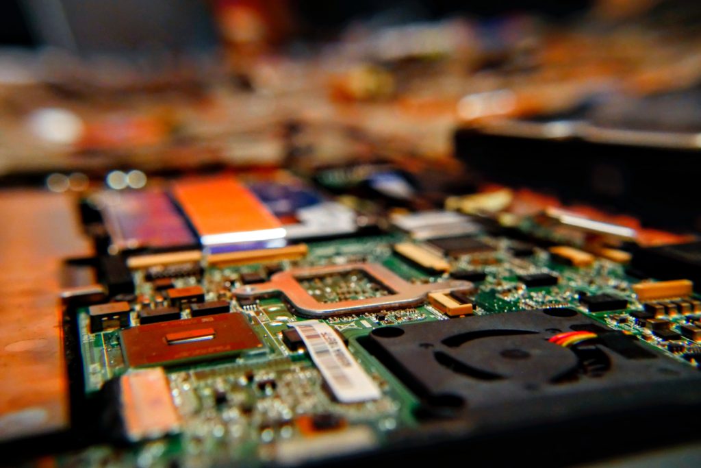
Photo by Laura Ockel on Unsplash
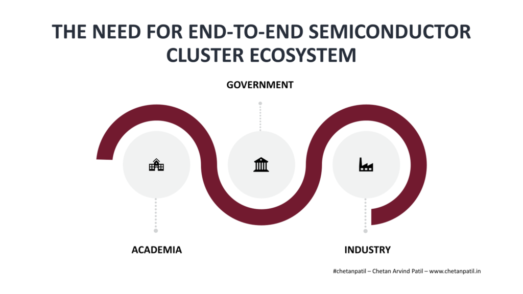
THE NEED FOR SEMICONDUCTOR POWERED XPU
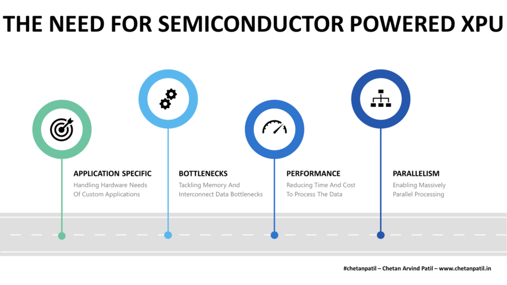
Every software application eventually has to get executed on a hardware system. Whether the software application is running on a smartphone or a data center, the data processing request has to get decoded (binary instructions) before the hardware system can process the request successfully. This seamless exchange of processes between software and hardware forms the base for a computer system.
Software form factor, user interface, and the speed might have changed over the years. However, the need to have a processing unit that can execute all the software code has not. Over the last two decades, the de-facto processing unit – the Central Processing Unit (CPU) – has seen several semiconductor and computer architecture backed technological advancement, that has taken computing to the next level.
As the software layers (application, presentation, session, and transport) are becoming model-driven (more pro-active, than re-active), so is the need to process the unique data/compute/memory intensive requests at the hardware-level.
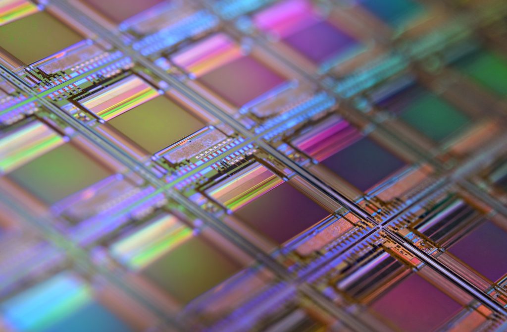
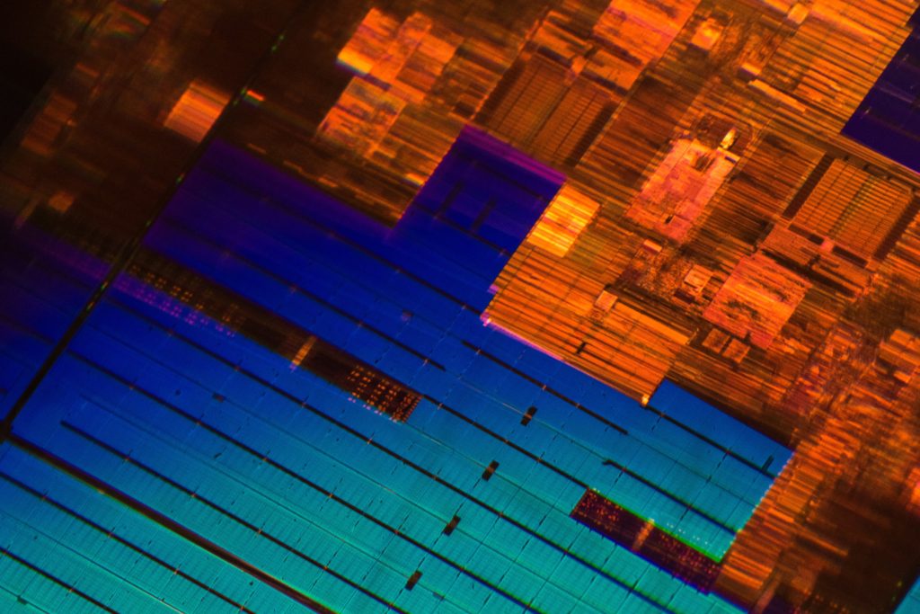
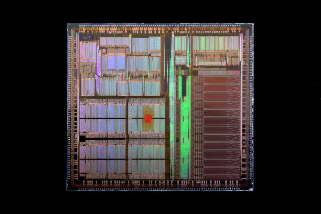
Traditional CPU earlier was designed to handle a single request at a time. Then, the computing world moved towards multi-CPU (multi-cores) to cater to the parallel computing demand. Today, the de-facto is a System-On-A-Chip (SoC) that packs the CPU, the Graphics Processing Unit (GPU), and other processing units to process the high-resolution, high-speed, highly-data intensively requests in the shortest possible time.
Semiconductor Powered XPU (X Processing Unit) Are More Application-Specific Than General-Purpose
The integrated system (mainly CPU + GPU on an SoC) has not been able to keep up with the computing world’s data processing demand. It has pushed the computer architects to design new types of processing units (apart from high-bandwidth memory, cache coherence, and smarter interconnect topology) that are more application-specific than general-purpose.
This race to come up with the new type of processing units has given rise to XPU:
- X = Application Domain — Vision, Graphic, Neural, X-Reality, Video, Audio, and so on
- P = Processing
- U = Unit
XPU is different than CPU and GPU as it caters to the specific needs of the application. XPU is more application-specific, and it can work standalone or as a co-processor/co-unit alongside the CPU and GPU. XPU is geared towards throughput and speedy data management that takes the best out of the CPU and GPU design methodology to enable application-specific needs. XPU is not only Application-Specific Integrated Circuit (ASIC) due to the workload it is designed to cater to, but can also be classified as Application-Specific Standard Product (ASSP).
The rise of XPU is enabling a new era in computing. The hardware and the semiconductor market are enjoying different challenges and solutions the XPU brings. Intel is betting big on it, and so is AMD. Apart from these two semiconductor giants, there are numerous innovative startups (and academic research) that have XPU powered solutions and are pushing the computing industry towards next-gen data processing.
Several types of XPU are available. It is vital to understand how these differ from each other apart from the two processing giants – the CPU and the GPU.
THE XPU CATALOG
There are numerous XPU powered examples in the market. Many of these are still in a nascent stage and yet to prove the solution in the market. Given the growth and demand for new AI workloads, the XPU catalog will keep growing.
Below are the major semiconductor powered XPU:
AIPU – AI Processing Unit — AIPU is targeted towards an Artificial Intelligence solution and is mainly designed to cater to the Edge AI market. MediaTek Helio series of SoC is an example of AIPU integrated with CPU and GPU. Even RAIP – Real AI Processing Unit (RAIPU), IPU – Intelligence Processing Unit or Image Processing Unit, EPU – Emotion Processing Unit – fall under IPU with the only difference being the change of name. The goal of AIPU, RAIPU, EPU, and IPU is the same – to process data to make a decision that is at-level or at-part with human intelligence.
APU – Accelerated Processing Unit — APU design requires fusing the CPU and GPU into a single die. AMD’s A-Series processor is a perfect example of an APU. APU is also capable of running a heterogeneous system by utilizing system-level architecture and software features.
AMPU – Analog Matrix Processing Unit — AMPU is designed to cater to the data training needs that are often large parameters that execute multiple matrix multiplications. AMPU custom feature to handle such parameters and matrix operations allows speedy training without relying on the external memory. MYTHIC’s Analog Matrix Processor is an example of AMPU.
BPU – Brain Processing Unit — BPU is envisioned to minim the human brain as it is. The processing unit is capable of performing multiple TOPS. Horizon’s Journey line of products is considered the first BPU ever and is designed in close collaboration with the Baidu Institute of Deep Learning. BPU may also form the base for Level 5 automation.
CPU – Central Processing Unit — CPU is the de-facto processing unit and is vital for general to specific purpose computing needs. Intel and AMD are leading the CPU innovation along with ARM. CPU is here to stay and will keep providing the much-needed multi-tasking capability for consumer applications. On top, Academia is still engaging in research to make cache and data pipeline more energy efficient.
DPU – Dataflow Processing Unit | Data Processing Unit | Data Parallel Unit — DPU focuses on speeding up the data movement between the cores and the memory. It requires a new interconnect topology apart from the smart placement of sub-blocks to minimize bottlenecks. The instruction set allows for faster memory and compute-intensive processing. Intel already several RISC (AVX512) instructions set to optimize processing for x64. DPU takes it to the next level with its highly optimized data pipeline, which enables massive parallelism. Fungible’s DPU is one such example apart from Deep Vision’s ARA series. RDPU – Reconfigurable Dataflow Processing Unit – is also a type of DPU.
DLPU – Deep Learning Processing Unit — A DLPU finds similarity with DPU. It is a domain-specific solution to enable faster training. DLPU finds use in Edge AI and similar applications. Researchers first showcase DLPU with DianNao paper, and recently in Cambricon-F paper.
GPU – Graphics Processing Unit – Like CPU, GPU has been in the market for a long time and is designed to cater to graphics applications. In the last few years, GPU has also found its way into AI/ML/DL applications too. Highly parallel design (with multiple core and large memory) of GPUs enables faster computation. GPU’s efficient programmability also allows faster training of dataset. NVIDIA by far is the leader in the GPU domain along with AMD, which is not far behind. Depending on how the GPU is fabricated in the computer system, it also gets classified as = DGPU – Discrete Graphic Processing Unit, GPGPU – General Purpose Graphic Processing Unit, EGPU – External Graphic Processing Unit, IGPU – Integrated Graphic Processing Unit.
HPU – Holographic Processing Unit — Coming out of Microsoft, HPU is designed for X-Reality. It incorporates design to process rich information that is generated by the sensors and cameras on the X-Reality device. HPU incorporates processing units to implement DNNs.
MCPU – Micro Controller Processing Unit — MCPU is not used to run operating systems or frameworks, but instead are geared to run Real-Time Operating System (RTOS) powered solution. MCPU find use in automotive, remote devices and even laptops desktop to offload non-critical tasks. ARM, Texas Instruments, and others have been providing MCPU solutions for a few decades. In the AI-powered world, the solution around MCPU is increasing, and architecture design is adapting to it.
NPU – Neural Processing Unit — NPU implements all the required blocks to enable faster data modeling using neural networks. Alibaba’s Ali-NPU is one such example. There are different types of NPU: NDPU – Neural Decision Processing Unit, NNPU – Neural Network Processing Unit, NDPU – Neural Decision Processing Unit. Eventually, the end-goal of the types of NPUs is the same – train the data faster using a neural network and framework.
PPU – Physics Processing Unit — Mostly used in an academic environment, PPU is designed using FPGA to provide an architecture that can enable faster simulations. SPARTA – SPARTA: Simulation of Physics on a Real-Time Architecture- the project was the first to design a PPU. Then, Ageia (later acquired by NVIDIA) also attempted to provide PPU solutions by providing architecture benefits at the arithmetic logic unit (ALU) level. Intel Xeon Phi, PlayStation 2’s VU0, and even GPUs are a type of PPU.
QPU – Quantum Processing Unit — QPU is a computational unit that uses quantum computing principles to perform a task. The physics used in QPU is drastically different than the general-purpose CPU. D-Wave Systems is the leader in QPU, and their QPU follows superconducting computing. Google, IBM, and Intel have QPU based on a quantum circuit. QPU is massive and not designed for mass-market and are supposed to compete against AIPU.
SPU – Streaming Processing Unit — SPU is useful to process streamed data. The structured data enables placing the cores and memory to minimize the delay in bringing the new data to process. Google’s TSPU – Tensor Streaming Processing Unit – is an example of SPU. There are different types of SPU available in the market apart from TSPU: GSPU – Graph Streaming Processing Unit, TMPU – Texture Mapping Processing Unit, TPU – Tensor Processing Unit
VPU – Vision/Visual/Video Processing Unit — VPU is coming out in the market due to the demand for providing a rich visual experience. VPU consists of more video encoding and decoding units to enabled faster 3D processing. X-Reality is an application area where VPU finds use. Intel’s Movidius VPU is a perfect example of how to use processing units to process video applications with low-latency.
WSPU – Wafer Scale Processing Unit — WSPU makes use of a full wafer to create single processing units instead of fabricated dies to develop processing units. Trilogy Systems was one of the first companies to provide such a solution. Recently, Cerebras has taken the lead and provide a workable deep learning solution using wafer-scale integration that shows how full wafer can be elegantly used to provide
With the growing need to process data faster and efficiently, the demand for semiconductor-powered unique XPU will keep growing.
THE CHALLENGES FOR SEMICONDUCTOR POWERED XPU
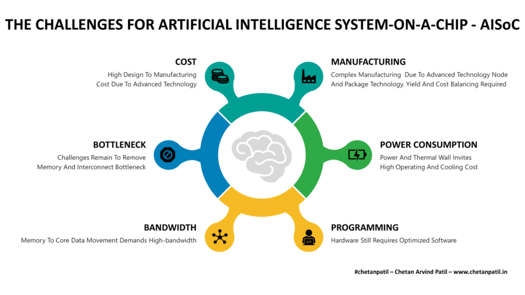
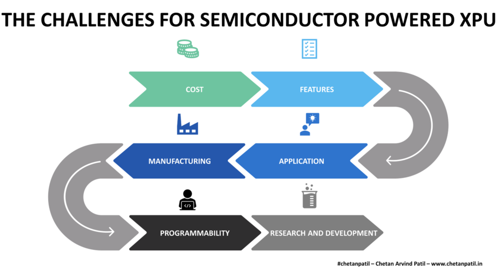
XPU is unique and solves niche problems. The challenges that come with it are many. Below are the hurdles and challenges that the semiconductor powered XPU face:
Cost: Designing a new processing unit not only enables new features to run the workload in the most optimized way possible. But it also adds the cost of design, development, and manufacturing. Balancing the CapEx is always the de-facto goal of any organization, and in the case of XPU, the stakes are higher given the stiff market competition. Companies looking to come out with more XPU based designs and solutions will have to make the process cost-effective to breakeven faster.
Features: XPU is feature-specific. Deciding which problem the XPU is going to solve is difficult to find. The semiconductor industry has launched different types of XPU that cater to almost all the possible computing domains and problems possible. Upcoming XPU will have to beat the existing XPU not only from the design point of view but also with respect to the features that make the new XPU sustainable in terms of power, performance, area, and cost.
Application: Defining use cases and features for XPU is another challenge. It requires figuring out the bottleneck in the existing applications/workloads and then designing the solution at the silicon level to solve it. TSU is one such example, which removes the bottleneck to train the data. Such a unique feature-based XPU is going to make it stand out in the market.
XPU Will Drive Innovation Along With General-Purpose Processing Units
Manufacturing: XPU either needs to be fabricated along with the CPU or as another block with the CPU inside the SoC or as a separate co-processing unit. In any of the three cases, it takes a unique semiconductor manufacturing process to ensure there is no process, quality, package, and reliability issues. Multi-Die Multi-Chip powered chiplets can be one way to ensure future XPU designs for manufacturability. The technology node and the packaging technology needs to be thoroughly tested before making the XPU with it. The goal of reducing the cost of manufacturing for XPU will be another challenge.
Programmability: Hardware is designed to run the software. Developing and running applications on any piece of silicon (mainly those designed to run operating systems and frameworks) requires the support of system-level libraries to ensure the data being processed can make use of all the internal features. Semiconductor companies developing different types of XPUs will have to provide APIs and system-level hardware interface libraries. This requires time and cost to develop. To keep developers engaged dedicated continuous API development teams are required. Providing such software features is vital and also a challenge to the XPU design team.
Research And Development: Continuous R&D is a vital factor that leads to a new type of XPU. It is critical to ensure that the R&D team can collaborate with academia to innovate new processing blocks. Organizing a dedicated top-notch R&D team is still a challenge given the competition in the semiconductor industry. Investment is another differentiating criteria when it comes to advancing new XPU designs.
It is an exciting time to be in the XPU domain. General-purpose CPU and GPU are here to stay, and along with XPU will enable a new, powerful and efficient way to solve the data problems.
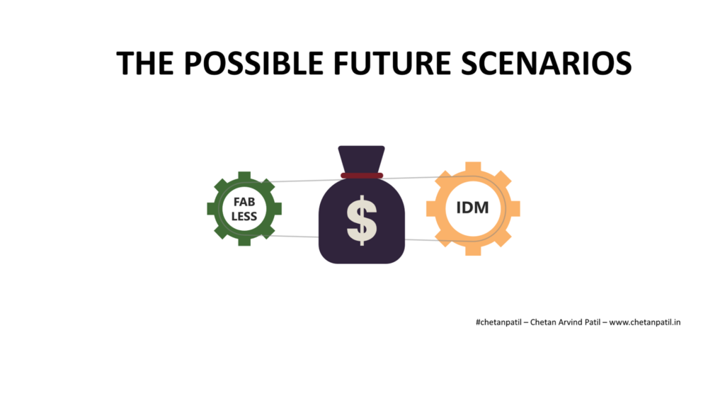
However, the need to innovate in the competitive semiconductor industry will be the race to watch out. Companies like Intel, Apple, AMD, Microsoft, Google, Amazon, and Facebook will play a crucial role in pushing the market for semiconductor powered XPU solutions, alongside promising FAB-LESS startups worldwide.