Blog

  • The Impact Of Semiconductor Equipment Shortage On Roadmap

    Image Generated Using 4o


    What Is Happening?

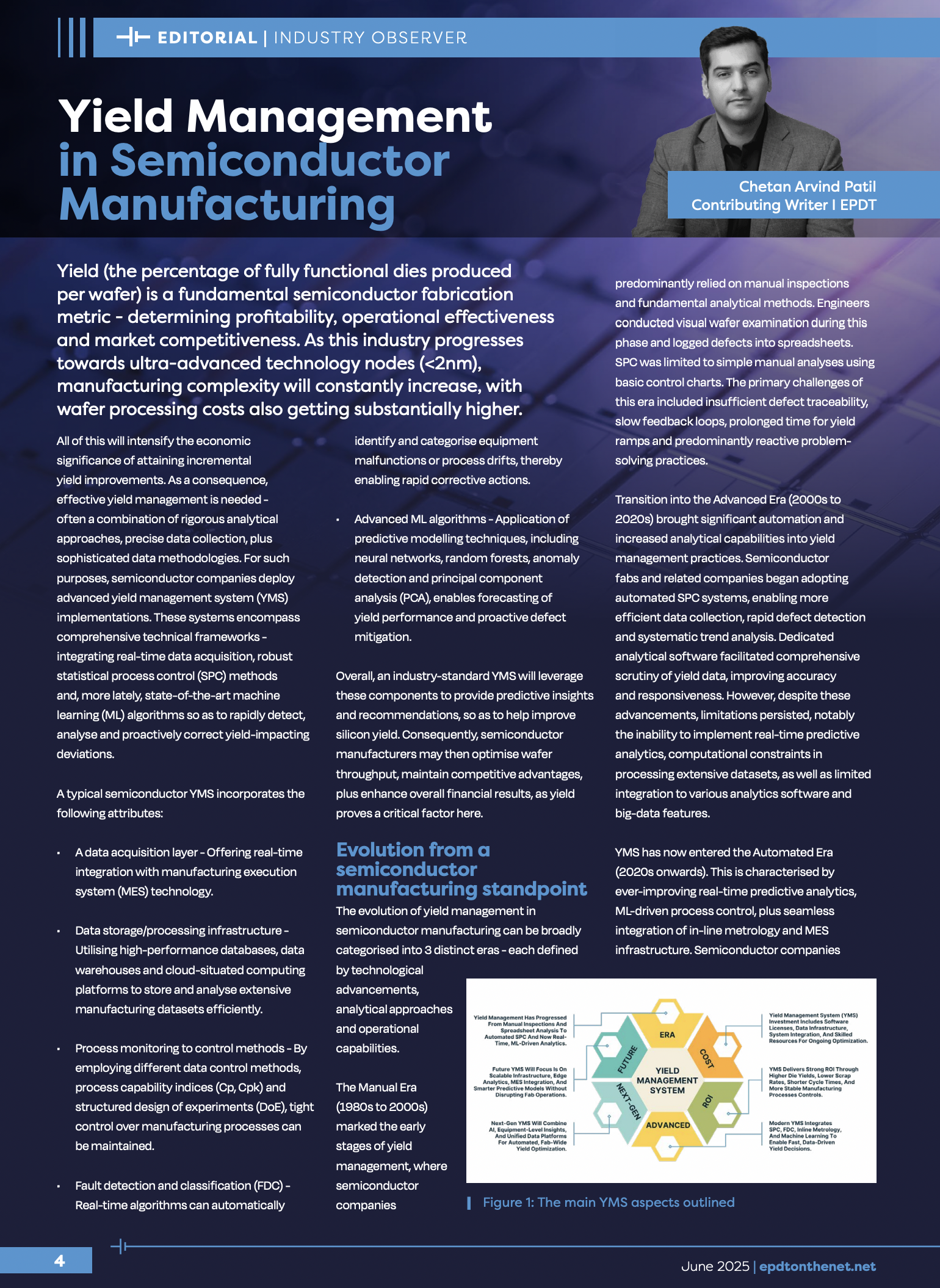
    The semiconductor industry has always grappled grappling with a persistent and intensifying equipment shortage. What began as a supply chain issue has now become a long-term structural constraint.

    Lead times for advanced manufacturing tools, particularly those essential for next-generation process nodes, have extended to 12 to 18 months or more. At the same time, even equipment supporting mature technologies, such as 200 mm wafer processing, is experiencing delays.

    This highlights the broad and systemic nature of the problem.


    Why Equipment Shortage Becomes A Big Deal?

    Semiconductor manufacturing is deeply dependent on a highly specialized class of equipment. Unlike general-purpose tools, these machines are purpose-built, node-specific, and often come from a limited number of suppliers.

    When lead times stretch or tool availability drops, it directly impacts the ability of fabs to maintain their roadmap, yield, quality, and, ultimately, time-to-market. In short, the flow of innovation slows down not due to a lack of design capability but due to the absence of critical hardware.

    Furthermore, the complexity of modern fabs exacerbates this challenge. A high-volume production line for advanced nodes may require more than hundreds of different tools across lithography, etch, deposition, metrology, CMP, and packaging.

    These tools are not interchangeable and must be qualified together to maintain process integrity. When even one tool is delayed, it can stall an entire line, creating cascading effects across production schedules, R&D timelines, and customer commitments.

    Let us take a look at the key reasons why equipment shortage disrupts semiconductor manufacturing:

    AspectImpact Due To Shortage
    Tool ComplexityAdvanced tools require long design and qualification cycles. Shortages cannot be solved quickly.
    Limited SuppliersMany equipment types are produced by only one or two vendors globally.
    Node-Specific DependencyTools are tightly coupled with process nodes. Older tools cannot support new technology nodes.
    Qualification TimeTool installation is not enough, process tuning and validation take months.
    Cascade DelaysDelay of one tool stalls entire production flow, affecting capacity and delivery.
    Capital InflexibilityTool purchases involve long-term planning and capital allocation. Reacting fast is difficult.
    Customer CommitmentsOEMs cannot meet chip demand, leading to missed product launch windows.

    Eventually, with so much at stake, the absence of even a single critical tool can delay an entire roadmap, impacting everything from process migration to end-product delivery in data centers, smartphones, the automotive industry, and beyond.


    How It Impacts Process To Product Roadmaps?

    In the semiconductor industry, process development and product introduction are tightly interlinked. The process defines the physical capability. The product determines the commercial outcome. When equipment is delayed, both timelines are disrupted, affecting yield learning, PDK maturity, product qualification, and volume scalability.

    A shortage of critical tools delays the start of process integration, slows down line bring-up, and reduces wafer availability for early silicon validation. This means that design teams working on cutting-edge products cannot access silicon when expected, pushing out verification cycles, delaying firmware and software stack development, and ultimately affecting go-to-market-to-market schedules.

    Roadmap PhaseDisruption Due to Equipment Shortage
    Process Development (RnD)Inability to start integration due to missing litho/metrology/etch tools.
    PDK ReleaseDelays in baseline silicon characterization slow down PDK delivery to design teams.
    First Silicon AvailabilityFewer tools → fewer wafers → delays in prototype chips.
    Design Verification And DebugLack of wafers hampers test chip data collection and corner validation.
    Yield LearningLimited data slows defect analysis, process tuning, and model refinement.
    Ramp To ProductionLine qualification cannot proceed on schedule, impacting customer commitments.
    Customer Product RoadmapsEnd customers delay their platform or system-level releases due to unavailable chips.

    From a strategic standpoint, roadmap slippage caused by tool shortages has become a defining bottleneck. In the past, product schedules were gated by design complexity or mask cycle time.

    Today, it is common to see entire process families stalled at 90 or 95 percent readiness, waiting not on tape-out but on tool delivery, installation, and qualification. This shift redefines time-to-market planning across the industry.


    What To Expect And How To Mitigate Equipment Cycle Time Impact?

    The semiconductor industry should expect prolonged equipment lead times well into 2026, driven by persistent supply constraints, including a constant increase in demand for high-tech processes using advanced computing solutions for new-age workloads. Even with record levels of capital investment, manufacturing capacity at the equipment level cannot scale instantly.

    This creates a new normal where tool delivery timelines must be considered a core constraint in both process development and product planning. The traditional assumption that capital expenditure translates directly into immediate equipment availability is no longer valid.

    To mitigate this impact, companies should adopt a mix of strategic and operational responses. These include placing multi-year tool orders, pre-qualifying process steps across multiple sites, and using virtual process modeling to reduce dependency on physical wafers in early development.

    Most critically, close alignment between fab teams and end customers will be essential, ensuring that roadmap changes driven by equipment constraints are communicated and absorbed early in the product planning cycle.


  • The Productization Cycle Time In Semiconductor Development

    Image Generated Using 4o


    What Is Semiconductor Productization Cycle Time?

    Semiconductor productization cycle time refers to the total duration required to transform a completed chip design into a fully qualified, production-ready product. It begins after the design is taped out and ends when the product is released to high-volume manufacturing with acceptable yield, quality, and system-level reliability. This period involves intensive cross-functional collaboration across silicon engineering, packaging, test development, validation, reliability, and supply chain.

    The cycle is not a single step but a structured series of technical handoffs, optimizations, and problem-solving phases. Each contributes to overall time-to-market and has a direct impact on cost, quality, and revenue generation.

    The key components of the productization cycle include:

    • Tapeout to first silicon readiness
    • Initial bring up and functional debug
    • ATE test program development and correlation
    • Package and assembly qualification
    • Reliability and standards-based qualification testing
    • Yield analysis and production ramp
    • Customer validation and system integration feedback

    Depending on the complexity of the product and the target market, this cycle can range from six months to over a year. Shortening the cycle without compromising quality is often a strategic priority, especially in competitive or regulated markets.

    In the long-term, managing this time effectively is what differentiates strong product execution from delayed or over-budget programs.


    Typical Timeline Of The Productization Cycle

    The productization cycle consists of several tightly coupled stages. Each stage has its own objectives, deliverables, and potential bottlenecks. While exact timelines vary depending on product complexity, market segment, and technology node, the typical range for a complete cycle is six to twelve months.

    The timeline below outlines each primary phase, its expected duration, and the core activities associated with it.

    StageEstimated DurationKey Activities
    First Silicon Readiness4 to 6 weeksTapeout to wafer delivery, packaging for evaluation
    Silicon Bringup2 to 6 weeksBasic functionality, register access, debug loops
    Test Program Development8 to 12 weeksATE pattern creation, DFT validation, test coverage
    Package Assembly4 to 6 weeksSubstrate readiness, thermal and form factor checks
    Reliability Qualification6 to 12 weeksHTOL, HAST, Temp Cycle, ESD, latch-up tests
    Yield Ramp and Optimization8 to 16 weeksProcess tuning, guardband validation, corner lots
    Customer Validation4 to 8 weeksApplication-level tests, system integration

    In many cases, some stages run in parallel to save time. For example, reliability testing and test program optimization may proceed concurrently after bringup. However, any failure in these parallel flows can lead to rework, which resets the clock for the affected stage.

    Thus, efficient productization requires not only strong technical execution but also program-level coordination to ensure each stage feeds smoothly into the next. Such a structure becomes even more critical when managing tape-outs across multiple products or process nodes.


    What Drives Productization Delays

    Delays in the productization cycle are common due to the technical complexity and cross-functional nature of semiconductor development. Common causes of delay include:

    • Incomplete Pre-Silicon Validation: Simulation fails to capture real-world corner cases that emerge only during bring-up
    • DFT and ATE Mismatch: Poor alignment between design-for-test features and test platform implementation slows test development
    • Packaging Issues: Packages may face late-stage problems with thermal, mechanical, or signal integrity
    • Qualification Failures: Reliability tests, such as HTOL or HAST, can fail, requiring debugging and retesting cycles
    • Yield Instability: Low or inconsistent yield across corners demands additional tuning and analysis
    • System-Level Gaps: Customer-side failures frequently result in late changes to silicon or test programs

    Even with detailed planning, issues often emerge from immature designs, process variability, and misaligned engineering handoffs.


    How Cycle Time Impacts Cost

    The productization cycle time has a direct impact on development costs. Each added week increases engineering effort, lab usage, and the need for additional silicon or packaging builds.

    These costs rise rapidly, especially for complex System-on-Chip (SoC) designs or high-reliability products. These longer cycles also stretch budgets and delay production, reducing the time available to recover investment.

    Delays also create opportunity costs. Missing key market windows or customer ramps can result in lost sales opportunities, lower selling prices, or even canceled projects.

    Underutilized equipment and late delivery in regulated markets may also trigger penalties. Managing cycle time effectively is essential for both technical execution and business success.


    Strategies To Optimize Productization Time

    Reducing productization cycle time requires more than just faster execution. It requires a structured, cross-functional approach that addresses bottlenecks, enhances handoff efficiency, and anticipates familiar sources of delay. Leading semiconductor companies treat productization as a tightly managed engineering flow, where technical readiness is synchronized with program planning and customer engagement. By front-loading risk and parallelizing key activities, teams can compress timelines without sacrificing quality or reliability.

    Below are the strategies to optimize productization time include:

    StrategyDescription
    Early Test DevelopmentBegin ATE pattern development and validation before first silicon using virtual test setups and simulations.
    First-Time-Right Design CultureEmphasize high-quality closure throughout the design cycle using linting, static checks, and sign-off tools to reduce post-silicon issues.
    Cross-Functional OwnershipAssign dedicated ownership early in the cycle to coordinate activities across design, test, validation, packaging, and customer engagement.
    Parallel Qualification and DebugRun reliability testing and test debug in parallel with early silicon to minimize serial dependencies.
    Unified Pre and Post-Silicon FlowAlign pre-silicon simulation environments with production test platforms to improve correlation and reduce transition time.
    Strong Data InfrastructureUse analytics tools for yield, failure analysis, and traceability to support faster debugging and feedback.
    Supplier and Customer IntegrationEngage OSATs, substrate vendors, and customers early to align requirements, timelines, and failure response plans.

    When these strategies are executed with discipline and data-driven feedback loops, teams can reduce cycle time significantly while improving first-pass success rates.

    Eventually, the result is not only faster product release but also greater cost control and more substantial customer confidence.


  • Semiconductor Supply Chain Ecosystem – Complexity, Risks, And The Need For Security

    Published By: Data Security Council of India
    Date: June 2025
    Media Type: Online Media Website

  • The Semiconductor ASIC Versus SoC Design Reality On A Post-Moore World

    Image Generated Using 4o


    What ASIC And SoC Actually Mean Today

    An ASIC was a fixed-function chip logic designed from scratch, optimized for area, power, and speed, and then locked down. It worked particularly well for high-volume products, where every bit of efficiency mattered.

    A System-On-A-Chip (SoC) integrates multiple functions, including CPU, memory controllers, accelerators, and I/Os, using pre-verified IP blocks. It reduced design time but gave up some control.

    The question is no longer “Is it an ASIC or SoC?” It is:

    • How much of it is reused?
    • How configurable is it?
    • How much control do you have?
    • Can team handle the integration and bring it up to speed?

    That line is now blurred. Most ASICs use third-party IPs. Some System-On-A-Chip (SoC) devices are heavily customized for specific applications. And hybrids, such as semi-custom SoCs and chiplet-based designs, mix both worlds.


    Design Tradeoffs: Cost, Time, And Risk

    The core difference between ASIC and SoC design is not technical. It is about tradeoffs. Engineering teams rarely get unlimited time, budget, or people. Every decision shifts pressure to another part of the process, resulting in more integration, extended verification, higher costs, or added schedule risk.

    ASICs and SoCs have different profiles in terms of cost structure, development time, silicon risk, and maintainability. These factors are not always apparent at the outset, especially when decision-makers prioritize performance or BOM reduction.

    The table below outlines the practical differences most teams encounter:

    FactorASIC DesignSoC Design
    Development Cost (NRE)High — Full RTL, physical design, verificationModerate — Uses licensed IPs and reference subsystems
    Licensing CostLow — Mostly in-house logicHigh — Paid IP cores (CPU, GPU, I/O, etc.)
    Time to MarketLong — Custom design and verification cycleShorter — Integration-focused, often platform-based
    Performance TuningHigh — Full control over timing and layoutLimited — IP black-box behavior restricts optimization
    Verification LoadFocused — Single-purpose, scoped verificationHeavy — Complex IP interactions and corner cases
    Risk of Re-spinHigh — Full custom logic, harder to catch bugsMedium — IP is usually well-tested but integration is risky
    Volume SuitabilityHigh — Payback improves with high unitsGood — Better for mid-volume or evolving product lines
    Design ReuseLow — Hard to adapt without major reworkHigh — Easier to reuse across multiple designs
    Team Skill RequirementAdvanced — Needs strong physical + logic teamMixed — Strong integration and system-level thinking
    Tooling/EDA DependencyHeavy — Full flow needed (RTL to GDSII)Shared — Platform vendors often provide part of toolchain

    Many teams attempt to strike a balance between the two, utilizing ASIC methodology for the core logic and incorporating SoC-style IP blocks around it. The key is not just choosing a design model but also knowing what your team can realistically deliver, verify, and provide production support for. Cost, time, and risk are always connected, improving one usually stresses the others.


    Post-Moore Constraints Are Changing The Game

    Shrinking nodes no longer guarantee better power, area, or speed. At 5nm and below, power density, interconnect delay, and thermal issues dominate. Routing is more challenging, and physical limits, such as variation and IR drop, can hinder performance gains.

    For ASICs, even finely tuned blocks now face yield and manufacturability challenges. Full-custom is harder to justify unless volumes are high. Teams increasingly rely on hardened IPs and foundry-guided flows to stay within constraints.

    SoCs handle this better through the reuse of mature IP blocks, stable interconnects, and known thermal profiles, thereby reducing risk. However, flexibility is limited. You cannot continually optimize data paths or packaging to fit specific system needs.

    In the post-Moore era, design is now more about managing limits than pushing specs. What matters is not what performs best in theory but what yields, scales, and ships reliably.


    Choose What You Can Sustain, Not Just What You Can Build

    The ASIC vs SoC decision is less about architecture and more about lifecycle cost, verification effort, and team maturity. If your design requires tight control over timing, power, or area and you have the resources to manage full RTL ownership, physical implementation, and signoff, ASIC can make sense.

    But every decision is expensive to change. One late bug or corner-case miss can delay the tape out or force a re-spin.

    SoCs reduce that risk by leveraging proven IP and platform integration. You trade off flexibility for predictability. But even that path demands strong system validation skills, especially when IP vendors vary in quality, methodology, and update cadence.

    The fundamental constraint is not what you can design, but rather what you can verify, debug, yield, and support under actual time and budget pressure. In a post-Moore landscape defined by complexity, cost, and uncertainty, sustainable execution beats architectural ambition. Choose accordingly.


  • Yield Management In Semiconductor Manufacturing

    Published By: Electronics Product Design And Test
    Date: June 2025
    Media Type: Online Media Website And Digital Magazine

  • Yield Management In Semiconductor Manufacturing

    Published By: Electronics Product Design And Test
    Date: June 2025
    Media Type: Online Media Website And Digital Magazine

  • The Semiconductor Learning Path – Build Your Own Roadmap Into the Industry

    Image Generated Using 4o


    Learning To Learn About The Semiconductor Industry

    The semiconductor industry is a maze of ideas, technologies, and challenges, an intersection of physics, chemistry, engineering, economics, and geopolitics.

    For an early engineer, it is easy to get lost in the details. Thus, how do you even begin to make sense of it all? What do you need to know? Where do you find the correct information? And how do you build fundamental skills that matter?

    It is not a field that can be mastered by simply reading a textbook. Learning about semiconductors is a process of learning how to learn, gathering knowledge from different domains, connecting dots across disciplines, and constantly adapting to new technologies and industry shifts.

    Let us explore how to build your roadmap into the semiconductor industry, enabling you to go beyond surface-level learning and develop real, practical expertise.


    Start With Curiosity And See The Big Picture

    Before diving into specifics like FinFETs or EUV lithography, step back and ask: What makes semiconductors so important? Why is the world investing over $1 trillion by 2030 into this industry? And what problems are semiconductors trying to solve today and in the future?

    As a beginner in this field, it is crucial first to understand the larger forces at play. What drives this industry? How do companies, countries, and technologies intersect? Why is there a global race to secure semiconductor supply chains? And how do these factors influence the way chips are designed, built, and tested?

    Let us break this down with a simple mental map:

    LayerFocus QuestionsExamples
    ApplicationsWhere are chips used?AI, automotive, smartphones, medical devices, etc
    Market ForcesWhat drives demand?AI workloads, EV growth, hyperscale data centers, consumer electronics, industrial automation
    Supply Chain & PolicyWho makes what, and where?Taiwan (TSMC: 55% of global foundry market), Korea (Samsung), US (Intel, Micron), Europe (ASML, Infineon), China (SMIC)
    Technical DomainsWhat are the core areas to learn?Design (EDA, architecture), fab (process tech, equipment), test (DFT, ATE), packaging (2.5D, 3D, chiplets)


    Where To Start Your Semiconductor Industry Learning and Exploration

    The semiconductor industry is not just a collection of devices and processes. It is a complex, global ecosystem driven by markets, applications, supply chains, and geopolitics. Understanding this broader context is crucial, as every technical decision, whether it involves a design feature, process node, or test method, ultimately ties back to it.

    That is why the first step in your learning journey is crucial. It should be to observe and map the landscape.

    This is about building awareness: Who are the key players? Where are the fabs? What are the dominant applications? How do global trends like AI, electric vehicles, and 6G impact chip demand? What bottlenecks and risks threaten the industry?

    It is essential to spend 1–2 months reading, watching, and listening, building a robust mental model of the industry before you dive into technical details. This preparation will give you the confidence to navigate the complexities of the semiconductor industry.

    Here is a table of recommended starting points to guide your exploration:

    ResourceWhat You’ll LearnLink
    SIA State of the Industry ReportsIndustry size, growth trends, global challengesSIA
    WSTS Market ForecastsRevenue by region, application, and nodeWSTS
    Deloitte & McKinsey Semiconductor OutlookMarket shifts, talent gaps, AI & EV demandDeloitte
    Tech Blogs (SemiWiki, EE Times, etc.)Real-world insights, design challenges, fab storiesSemiWiki
    Conference Keynotes (IEDM, DAC, SEMICON)Cutting-edge research, technology roadmapsIEDM, SEMICON

    Reading these sources is not about memorizing numbers or names, it is more about pattern recognition.

    For instance:

    • When you see that AI and automotive are driving new chip demand, you will understand why design teams are focusing on high-bandwidth memory and power efficiency.
    • When you read about foundry concentration in Taiwan and near-by region, you will grasp the geopolitical risks and supply chain vulnerabilities that shape investment decisions.
    • When you learn that testing and packaging costs can make or break profitability, you will appreciate why certain startups focus on advanced packaging solutions or automated test flows.

    This contextual knowledge will act as your anchor. It helps you ask better questions when you later study design, fabrication, or validation.

    For example: Why are specific nodes (e.g., 5nm, 3nm) so costly to manufacture? Why is there a shortage of skilled talent in fabs? Why are governments pouring billions into on-shoring chip production?

    The goal is not to become an expert in every domain yet, but to orient yourself in the industry’s landscape so that your future learning builds on a strong foundation.


    Understand The Core Technical Domains And The Building Blocks

    Once you have a big-picture view of the semiconductor industry, its applications, markets, and supply chain, it is time to dive into the technical core: how chips are built.

    Semiconductors are not just one thing, they are a blend of physics, materials, design, fabrication, testing, and packaging. You do not need to know everything, but you should develop a working understanding of these key areas.

    Start with device physics. Learn how materials like silicon conduct electricity, how transistors switch, and how scaling pushes limits. This is where everything in a chip begins.

    Move to process and fabrication. This is about how chips are physically constructed using tools such as lithography, etching, and deposition. You will understand why advanced nodes, such as 5 nanometers, are so challenging and why yield is a critical factor in production.

    Learn design and architecture. This is where logic becomes circuits, and circuits become chips. Whether it is writing RTL, simulating circuits, or understanding a system architecture, this knowledge connects ideas to real hardware.

    Finally, explore testing, validation, and packaging. Testing ensures that a chip works across all conditions, and packaging serves as the bridge between the silicon and the real world. With 3D stacking and chiplets on the rise, the packaging is no longer an afterthought, it has become an integral part of the system design itself.


    Stay Current, Follow Trends, Reports, And Community Insights

    The semiconductor industry is in constant motion, technologies evolve, markets shift, and policies reshape priorities. Staying relevant means more than just learning the basics once, it is about cultivating the habit of continuous learning.

    Follow market reports, read industry insights, and engage with the community. Build a system for tracking trends and questioning how they connect to the technical foundations you are learning.

    This mindset sets great engineers apart. The best in the field are not just experts in one area, they are curious, connected, and adaptable. They understand how technical decisions relate to market demands, how design influences testing, and how global events can shape the future of chips.

    Here are a few suggestions to help you stay on track:

    • Subscribe to industry newsletters like SIA, Semiconductor Digest, EPDT, and WSTS. They will help you keep up with market data, reports, and policy updates
    • Attend webinars and technical talks; even one session a month from conferences like IEDM, DAC, or SEMICON can provide valuable insights
    • Follow semiconductor engineers and thought leaders on LinkedIn, people who share real-world problems, industry trends, and project breakdowns
    • Set a routine: Dedicate 30 minutes a day or 2 hours a week to learning and reflection
    • Start small projects: Simulate circuits, reverse-engineer a teardown, or write a summary of a technical paper
    • Share your learning: Write a LinkedIn post or blog, explain a concept to a friend, or discuss it with peers. Teaching reinforces learning

    As you build your roadmap in the semiconductor world, remember to stay curious, stay connected, and stay learning.

    That is the only way to keep up in this fast-moving industry and to grow into a professional who not only understands how chips work but why they matter.


  • The Real Cost Of Scaling A Semiconductor Design From Prototype To Production

    Image Generated Using DALL-E


    Prototyping Is Not A Production

    Scaling a semiconductor design from prototype to production is where promising ideas meet harsh reality. A prototype demonstrates feasibility and shows that a concept can work under controlled conditions but is not a finished product. Many teams celebrate the first silicon success, only to realize later that this milestone marks the beginning of the journey to market, not the end.

    The challenges of scaling are often underestimated. At advanced nodes, a single complete mask set can cost upward of a million dollars. A seemingly minor design change, such as adjusting a clock buffer or modifying a pin assignment, can require a complete mask revision and push schedules back by several weeks.

    On the other hand, custom test boards, essential for silicon bring-up and debugging, often cost hundreds of thousands of dollars per iteration, depending on complexity. Then, the debug cycles after prototype validation, whether addressing signal integrity issues, timing violations, or power delivery concerns, can add four to eight weeks per iteration.

    Prototypes often rely on multi-project wafer shuttles to reduce early costs, but these shared runs offer only a limited view of production readiness. They do not reflect the true complexity of dedicated wafer starts, volume scaling, or the demands of final test and qualification. A prototype proves that a design can function in the lab but does not guarantee manufacturability, stable yield, or long-term reliability in a production environment.

    This gap between a working design and a shipping product is where the real cost of scaling is revealed.


    Cost Of Prototyping

    Prototyping is the first critical milestone in the semiconductor New Product Introduction (NPI) process. It is much more than demonstrating that a design works on paper. A prototype integrates silicon fabrication, hardware development, test program creation, and validation under real-world conditions.

    Each step introduces risk, consumes resources, and requires precise coordination. Early success with a prototype can create the impression that a design is ready for production, but this is often misleading.

    A functioning prototype does not ensure the design will meet yield, reliability, and manufacturability targets in volume. The complexity of scaling is frequently underestimated, leading to unexpected delays, rework cycles, and increased costs.

    ActivityTypical TimeframeCost Considerations
    Mask Set Development4 to 6 weeksHigh fixed cost per iteration
    Multi-Project Wafer (MPW) Shuttle3 to 4 months availabilityLower cost, limited production insight
    Test Board Design and Fabrication3 to 5 weeksMultiple iterations may be required
    ATE Test Program Development4 to 6 weeksTester time and engineering effort
    PVT Characterization3 to 5 weeksRequires multiple wafer lots
    Qualification (JEDEC, AEC)8 to 12 weeksFull wafer lots, package variants, and extended testing
    Debug and Correlation Cycles2 to 4 weeks per issueAdditional wafer use and test time

    The path from prototype to production demands a tightly managed flow that balances silicon development, board design, test engineering, and system validation. Minor design changes can trigger costly and time-consuming rework. At the same time, late-stage discoveries of signal integrity issues, timing violations, or power delivery challenges can set entire programs back by weeks or months.

    Prototypes typically rely on shared wafer shuttles and lab setups that do not reflect the realities of dedicated high-volume production. Without a robust plan for test coverage, validation, and correlation, teams risk entering production with incomplete knowledge of their design’s behavior.

    A successful prototype results from cross-functional alignment between design, hardware, and validation teams. When this coordination breaks down, the actual cost of prototyping reveals itself in missed schedules, strained budgets, and compromised product launches.


    Transitioning To Production

    Transitioning a semiconductor design from prototype to production is not a simple handoff. It is a complex, iterative process that requires carefully coordinating design teams, manufacturing partners, test engineers, and supply chain specialists.

    What works in a lab must now perform reliably across millions of units. This step demands a shift in mindset from optimizing for a single working chip to building a repeatable, scalable process that delivers consistent performance and yield.

    Production readiness hinges on a deep understanding of the entire flow. Foundry slots must be secured based on realistic forecasts, and wafer starts must align with packaging and test capacity. Any misalignment in this chain introduces delays that ripple across the schedule.

    For example, a late-stage design change can trigger a new mask spin, delay wafer starts, and require revalidation of test programs and packaging processes. Each step consumes time and resources, creating a compounding effect that can push out delivery timelines and strain customer relationships.

    Transitioning to production is not just about pushing more wafers through a fab. It is about building a reliable, predictable system that balances technical rigor with operational efficiency. Success at this stage determines whether a design remains an engineering milestone or becomes a commercially viable product.


    Takeaway

    Scaling a semiconductor design from prototype to production is a complex, multi-dimensional challenge. A design must not only work in a lab but also withstand the realities of high-volume manufacturing, tight supply chains, and demanding customer timelines.

    The costs and risks involved at each stage, from mask sets and test infrastructure to packaging yield and logistics, compound quickly. Small inefficiencies in yield or test throughput can multiply into significant financial losses when measured across millions of units.

    Success in semiconductor scaling is not the result of technical brilliance alone. It is built on operational discipline, proactive risk management, and cross-functional alignment across design, manufacturing, and supply chain teams.

    Teams that plan for the entire journey anticipate challenges and maintain a deep focus on execution, ultimately succeeding in turning innovative designs into commercially viable products.


  • The Semiconductor Product Is More Than Just Silicon

    Image Generated Using 4o


    Silicon Alone Is Not The Product

    Silicon is the centerpiece of semiconductor innovation, but a bare die is not a product. What comes out of a foundry is an ultra-thin, unprotected sliver of silicon that cannot survive real-world application environments. It lacks mechanical durability, electrical connectivity, and environmental protection. No system designer can solder a raw die onto a board or expose it to industrial use conditions without risking catastrophic failure. The die may contain billions of transistors, but it is inaccessible and incomplete without packaging and interface layers.

    The core reasons why silicon is not a finished product:

    • It has no standard interface: external signals cannot connect directly to on-die metal pads
    • It lacks mechanical protection: dies are prone to cracks, delamination, and ESD damage
    • It cannot be mounted: without packaging, there is no board-level attach mechanism
    • It is unvalidated: operation under real voltage, temperature, and timing corners remains unknown
    • It is unqualified: the die has not passed JEDEC, AEC-Q, or industry-required reliability screening

    More importantly, silicon alone does not deliver functionality. Modern chips require configuration, calibration, and system-level interaction before performing as intended. A die sitting in a tray does not regulate power, process data, or handle sensor input. It must be connected to the rest of the system through physical packaging, embedded firmware, and electrical integration. Without this infrastructure, it cannot support its intended use case, let alone pass reliability or performance qualification for commercial deployment.

    Ultimately, productization is the bridge between die-level innovation and the end application. Without it, silicon remains a prototype, not a deliverable. The success of a semiconductor product lies not just in its design but in its transformation into a manufacturable, testable, and deployable solution.


    Engineering Beyond Silicon

    Once the die is fabricated, a deeper engineering phase begins, determining whether the silicon can become a reliable, shippable product. This phase involves translating the raw electrical design into a complete physical and functional unit. It is not enough for the die to meet spec in simulation. It must meet spec in the real world, in every corner case, and under every stress condition. This requires a systematic collaboration between packaging engineers, test engineers, validation teams, and firmware developers.

    ComponentRole In Productization
    Package DesignDetermines IO routing, power integrity, and thermal dissipation
    Test Program DevelopmentDefines coverage, test limits, and pass/fail criteria for each silicon lot
    Validation InfrastructureEnsures functionality across PVT (Process, Voltage, Temperature) conditions
    Qualification PlanningMaps out JEDEC, AEC, or custom reliability tests over production lots
    Firmware And CalibrationBrings up the chip, configures subsystems, and ensures device consistency

    Yield, Cost, And Time

    Even if a chip functions correctly. The success as a product depends on three tightly linked constraints: yield, cost, and time.

    High-performance silicon that yields poorly or takes too long to qualify often becomes commercially unviable. Yield losses can occur at multiple stages, such as wafer fabrication, packaging, final test, and system-level integration.

    For example, fab defects, package delamination, or test escapes can all degrade the number of good units. At the same time, some failures only emerge under real-world operating conditions like voltage droop or thermal cycling.

    A product that yields at 70 percent must absorb that loss into cost, and even modest increases in test time can significantly impact margins at high volumes. Time is equally critical delays in validation or qualification can miss market windows, resulting in lost design wins.

    Many chips fail not because they lack functionality but because they cannot meet volume, cost, or launch deadlines. Managing yield, price, and time in semiconductor productization is not optional, it is fundamental to delivering a viable product.


    Thinking In Terms Of The Whole Product

    A successful semiconductor product is more than a functional die, it results from coordinated engineering across design, packaging, testing, validation, and firmware. Teams that treat tape out as the finish line often face downstream failures that could have been avoided with system-level foresight.

    For instance, an SoC with impressive PPA may fail thermal targets due to poor package planning or require silicon respin because debug visibility was not designed. The product mindset starts at architecture, where tradeoffs are made for spec achievement, robustness, yield, and deployment efficiency.

    This approach demands that design decisions anticipate real-world constraints: ATE test time limits, handler thermal profiles, firmware bring-up timelines, and qualification windows. It also requires validation environments that reflect actual system use, not just block-level correctness.

    Teams considering the whole product build an observability plan for field failures and close the loop between lab data and production metrics. They succeed by designing high-performing silicon and delivering repeatable, validated, and field-ready semiconductor solutions.


  • The U.S. Semiconductor Supply Chain – Now And The Future

    Image Generated Using 4o


    United States Semiconductor Industry

    The United States semiconductor industry has been foundational in shaping the modern digital world. From the invention of the integrated circuit to the articulation of Moore’s Law, the U.S. was instrumental in pioneering the core technologies that underpin global electronics today.

    However, as we enter 2025, the landscape has shifted. While the U.S. continues to lead in critical upstream segments, including chip design, electronic design automation (EDA), and semiconductor manufacturing equipment, much of its physical fabrication and packaging capability has migrated overseas over the course of last four decades. The result is a complex mix of strength in innovation and dependency in production.

    To understand the current position and emerging trajectory of the U.S. semiconductor supply chain, it is thus essential to examine it across four interdependent domains:

    1. Manufacturing And Packaging Capabilities
    2. Upstream Leadership: Equipment, EDA, And IP
    3. Policy, Industrial Strategy, And The CHIPS Act
    4. The Road Ahead: Building A Resilient And Competitive Future

    Each domain highlights not only the past’s legacy and limitations but also the strategic imperatives shaping the next chapter of U.S. semiconductor leadership.


    Manufacturing And Packaging Capabilities

    Over 80 percent of global semiconductor packaging is now carried out in Asia by Outsourced Semiconductor Assembly and Test (OSAT) providers. Although there are OSATs that are headquartered in the United States, most of its packaging (manufacturing plants) operations are based in Asian countries.

    Historically, the United States pioneered packaging technologies, from dual in-line packages to early wire bond methods. However, by the late 1990s, these labor-intensive processes had largely been offshored. Today, chips are designed in the U.S., and at the same time the fabrication is overseas and only returned as completed parts ready for system integration.

    This structural dependency is becoming more critical as the packaging itself transitions from a cost center to a performance enabler. The emergence of advanced packaging, such as 2.5D interposers, chiplet-based architectures, and three-dimensional stacking, redefines the backend’s role in overall system performance. These technologies address interconnect bottlenecks and enable heterogeneous integration that is no longer achievable by scaling transistors alone.

    Companies in the US are now leading efforts to push packaging beyond traditional boundaries. While few companies have build some domestic capability in this space, it does not yet match the high-volume, highly integrated ecosystems that many have developed in Asia.

    As chiplet-based designs become standard and system performance increasingly hinges on packaging innovation, this capability gap poses a strategic risk. Closing it will require capital investment and a coordinated build-out of ecosystem partners, precision tooling, and workforce expertise to support volume-scale, advanced backend manufacturing within the United States.


    Upstream Leadership: Equipment, EDA, And IP

    While the United States has experienced a gradual decline in its semiconductor manufacturing share, it continues to hold strategic leverage through its dominance in upstream segments of the supply chain. This includes leadership in semiconductor manufacturing equipment (SME), electronic design automation (EDA), and reusable intellectual property (IP), all of which are essential to the global semiconductor ecosystem.

    U.S. companies account for approximately 40 to 45 percent of the global SME market. Several US based key industry leaders are central in enabling deposition, etch, and metrology at the most advanced technology nodes. In addition to complete toolsets, U.S. component suppliers are deeply integrated into the global lithography ecosystem.

    The United States holds an even stronger position in the domain of EDA. U.S. companies collectively control nearly 90 percent of the global EDA software market. These tools are indispensable for chip design, logic verification, physical implementation, and yield optimization. No advanced integrated circuit can proceed to manufacturing without undergoing design validation and signoff using U.S.-origin software.

    This leadership extends further into the realm of silicon IP. From interface controllers and high-speed physical layer blocks to complete processor cores, U.S. companies provide a substantial portion of the reusable design building blocks used across the industry. These IP blocks are embedded in mobile systems-on-chip, data center processors, AI accelerators, and edge devices. This dominance in soft IP has created a form of control that, while less visible than fabrication or packaging, is deeply embedded in global product development.


    Policy, Industrial Strategy, And The CHIPS Act

    The sharp decline in the United States’ share of global semiconductor manufacturing, from 37 percent in 1990 to approximately 12 percent over decades, reflects more than just market trends. It highlights a long-standing policy imbalance, as several key Asian countries have consistently supported their domestic semiconductor sectors through targeted subsidies, infrastructure development, and coordinated industrial strategy.

    In contrast, the United States relied heavily on market forces, allowing manufacturing capacity and supply chain depth to shift overseas. The CHIPS and Science Act passed in 2022, marked a major policy correction by providing 52.7 billion dollars in federal incentives to stimulate new fabrication capacity, establish research centers, and support electronic design automation, materials development, and workforce training.

    Initial momentum has been significant, with more than 200 billion dollars in private investment already announced, including major fabrication projects several key platers in this space. Yet funding alone will not address the structural barriers that remain. The industry faces a pressing shortage of skilled workers, with projections indicating a need for over 100,000 additional professionals by 2030 across research, engineering, technical, and operational roles.

    At the same time, critical dependencies in materials, substrates, and packaging services persist, leaving even CHIPS-supported fabs reliant on imports. Delays due to permitting and construction constraints have also emerged. The CHIPS Act provides a vital foundation, but sustained execution, workforce development, and domestic supply chain expansion will be essential for long-term impact.


    The Road Ahead: Building A Resilient And Competitive Future

    As the U.S. semiconductor sector works to regain manufacturing depth, the path forward is not about replicating the past. It is about reshaping the future around new technological, economic, and geopolitical realities. Success will hinge on executing a focused strategy across four foundational areas:

    Strategic PillarDescriptionWhy It Matters
    Regional ResilienceShift from globalization dependence to a balanced ecosystem with strong domestic and allied regional capacity.Ensures continuity during global shocks and reduces single-point vulnerabilities.
    Technology LeadershipLead in post-Moore’s Law domains like chiplets, heterogeneous integration, and advanced packaging.Maintains U.S. leadership at the frontier of innovation where performance scaling now depends on integration.
    Supply Chain ReinforcementDevelop or secure access to critical inputs such as ultra-pure chemicals, substrates, OSAT capacity, and photomasks.Supports reliable fab operations and prevents bottlenecks in scaling domestic manufacturing.
    Workforce And EducationInvest in STEM education, technician training, and skilled immigration pipelines.Addresses the industry’s core labor bottleneck and ensures long-term innovation capacity.

    Rebuilding the U.S. semiconductor supply chain will require decades of coordinated investment and planning across policy, private enterprise, and education. By focusing on these four pillars, the U.S. has an opportunity not only to restore capability but also to redefine strategic, scalable, and resilient semiconductor leadership.