Blog

  • The Semiconductor Thermography Data

    Image Generated Using DALL-E


    Fundamental Concepts of Semiconductor Thermography

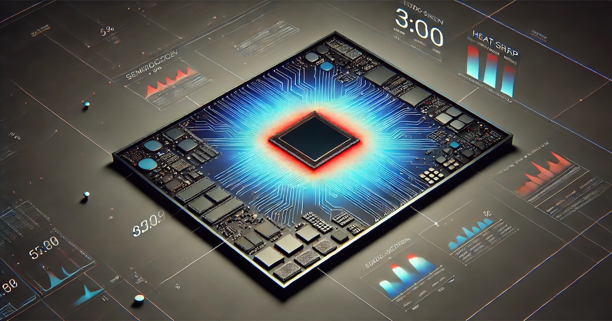
    Semiconductor thermography is a non-destructive measurement technique that quantifies and visualizes temperature variations within semiconductor devices, particularly Integrated Circuits (ICs). It primarily operates by detecting infrared (IR) emissions or other temperature-dependent physical changes at the device’s surface, allowing precise characterization of thermal behaviors.

    Thermography produces detailed thermal maps, accurately depicting temperature gradients, localized hotspots, and thermal anomalies undetectable by conventional electrical testing methods. These thermal maps are essential for identifying device areas experiencing elevated temperatures due to resistive losses (Joule heating), transistor switching activities, or leakage currents at advanced technology nodes.

    A critical parameter determined through thermography is the junction temperature (Tj), precisely the temperature at the semiconductor transistor junction level. Elevated junction temperatures directly reduce carrier mobility, negatively impacting transistor switching speeds and overall chip performance. Additionally, higher Tj accelerates device aging mechanisms such as electro-migration, Negative-Bias Temperature Instability (NBTI), Time-Dependent Dielectric Breakdown (TDDB), and Hot Carrier Injection (HCI), significantly reducing device reliability and lifespan.

    This, accurate thermographic measurement and interpretation allow semiconductor engineers to evaluate and optimize thermal management solutions, ensuring reliable device operation, improved performance, and extended operational lifetime.


    Industry-Accepted Thermography Techniques

    Accurately capturing and interpreting thermal behavior is crucial in the semiconductor industry. Over the past decades, several thermography techniques have been developed, each serving specific needs and practical scenarios.

    Below are the industry-standard thermography techniques widely recognized and adopted by semiconductor professionals.

    TechniqueOperating PrincipleAdvantagesLimitations & ConsiderationsTypical Applications
    Infrared (IR) ThermographyDetects infrared heat emitted by semiconductor surfaces to create thermal maps.– Non-contact and safe
    – Real-time monitoring
    – Widely available
    – Limited resolution at small nodes
    – Accuracy affected by surface properties
    – Production monitoring
    – Quick failure checks
    – Reliability tests
    Thermoreflectance ImagingMeasures temperature-induced changes in surface reflectivity using optical microscopy.– Very high spatial resolution
    – Precise quantitative data
    – Complex setup (lab-based)
    – Surface preparation critical
    – Advanced failure analysis
    – Research & development
    – Validation of complex designs
    Liquid Crystal ThermographyUses temperature-sensitive liquid crystals applied to surfaces, changing color with heat.– Intuitive visual heat mapping
    – Sensitive to small temperature variations
    – Requires direct contact
    – Limited temperature range
    – Unsuitable for packaged ICs
    – Lab visualization of thermal distribution
    – Prototype testing
    Fluorescent MicrothermographyApplies fluorescent dyes whose emission characteristics vary with temperature; observed microscopically.– High-detail thermal maps
    – Detects microscopic hotspots
    – Complex equipment
    – Invasive surface preparation
    – Detailed transistor-level analysis
    – R&D characterization
    Thermal Emission Microscopy (EMMI)Captures IR emissions from electrical defects (shorts, leaks) using specialized microscopy.– Precise defect localization
    – Non-destructive
    – Specialized lab conditions
    – Limited for broad-area thermal measurement
    – Automotive/industrial failure analysis
    – Returned device investigations
    Raman ThermographyUses Raman spectroscopy to detect temperature-dependent shifts in semiconductor materials.– High spatial resolution
    – Non-contact, precise measurements
    – Complex, expensive equipment
    – Specialized lab use only
    – Fundamental research
    – Precise material analysis
    Scanning Thermal Microscopy (SThM)Uses a heated micro-probe scanning across surfaces to detect local temperature variations.– Nanoscale resolution
    – Direct thermal conductivity measurements
    – Slow measurement speed
    – Potentially invasive contact
    – Research applications
    – Nanoscale heat analysis

    Each of these thermography technique has distinct strengths and limitations. The selection typically depends on practical considerations such as required spatial resolution, environment (production vs. lab), measurement accuracy, and the type of semiconductor device under analysis. Industry professionals must carefully evaluate these factors to ensure accurate thermal characterization and successful thermal management.


    Why Semiconductor Thermography Data

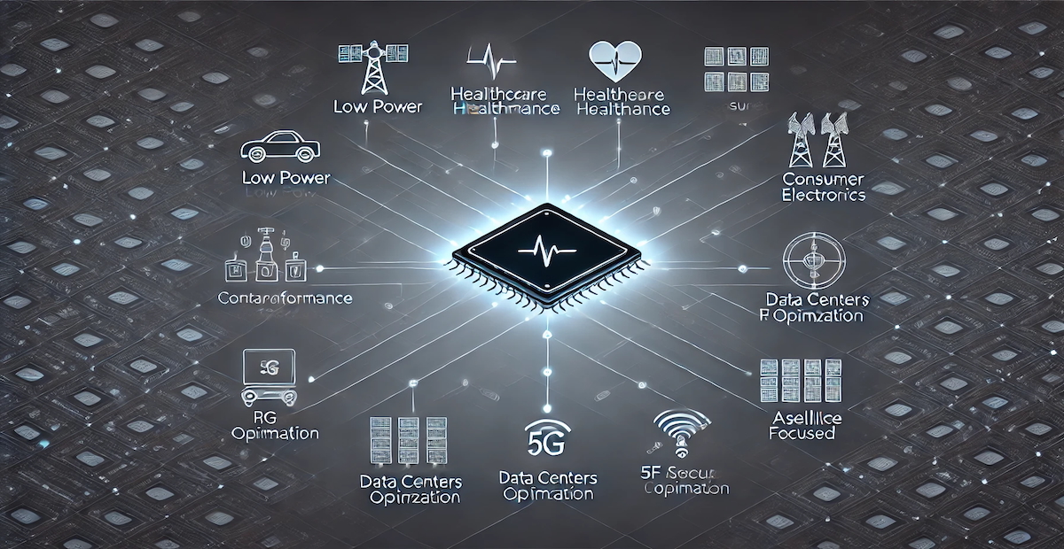
    Semiconductor thermography data provides detailed visibility into device thermal performance, making it indispensable for engineers across multiple phases of the semiconductor lifecycle.

    • Device Performance and Reliability: Thermography data shows the real thermal behavior of semiconductor devices. It helps engineers identify and fix heat-related performance issues, improving device reliability and lifespan.
    • Precision Failure Analysis: Thermography quickly locates subtle defects, such as leakage currents, short circuits, or electromigration, that are hard to detect with standard electrical tests alone.
    • Manufacturing Yield Improvement: Thermal imaging identifies manufacturing problems early, allowing quick corrections. This helps semiconductor companies reduce defects, improve yields, and save costs.
    • Compliance With Industry Standards: Thermal data ensures semiconductor devices meet critical industry standards (e.g., JEDEC, AEC-Q100, MIL-STD). This compliance is essential, especially in automotive, aerospace, and industrial electronics, where reliability is crucial.
    • Optimized Semiconductor Design: Thermography provides important feedback during chip design, helping engineers optimize transistor placement, power distribution, cooling methods, and packaging. This avoids expensive design revisions and speeds up development.
    • Cost Efficiency And Profitability: Identifying and solving thermal issues early saves money, improves product yields, and extends device lifetime. This makes semiconductor companies more competitive and profitable.

    By providing precise thermal insights, engineers can then address critical reliability and performance issues proactively.


    Future Techniques For Semiconductor Thermography

    Traditional thermography faces new challenges as semiconductor technology advances toward smaller, denser, and more complex chips. The industry is developing advanced methods to meet these demands, including high-resolution quantum-based sensors, integrated on-chip temperature monitoring, and hybrid diagnostic techniques.

    Future thermography will increasingly depend on sophisticated modeling techniques, which will provide accurate thermal simulations that closely replicate real-world operating conditions. However, these advanced models and analyses have higher computational costs, requiring significant computing resources and infrastructure.

    Additionally, accurately replicating real-system conditions, such as realistic power loads and thermal environments, will become critical. Achieving this realism adds complexity, increasing equipment and licensing costs for specialized software and hardware.

    Balancing precision, computational expense, real-system replication, and licensing fees will thus become crucial. The semiconductor industry must manage these trade-offs effectively to ensure that future thermography techniques remain practical and cost-efficient, ultimately safeguarding device reliability and performance.


  • The Role Of Simulation In Semiconductor Product Development

    Image Generated Using DALL-E


    Simulation In Semiconductor Development

    The semiconductor industry constantly evolves, increasing design complexity and high manufacturing costs. Traditional methods relied on physical prototyping and manual calculations, but as chips now contain billions of transistors, advanced simulation tools have become essential. Simulation allows engineers to test designs, predict performance, and optimize manufacturing processes before production, reducing risks and costs. Including electrical, thermal, and mechanical, providing a detailed view of semiconductor behavior before fabrication.

    Key roles played by simulation:

    • Cost Reduction: Detects design flaws early, minimizing expensive prototyping and reducing material waste
    • Time Efficiency: Enables rapid design iterations and scenario testing, accelerating time-to-market
    • Risk Mitigation: Simulates extreme conditions to identify potential reliability issues before production
    • Innovation Facilitation: Supports “what-if” scenarios, allowing engineers to push technology boundaries

    Simulation Techniques And Tools In Semiconductor Development

    As semiconductor devices become more advanced, specialized simulation methodologies ensure accurate design and efficient manufacturing. These simulations help engineers model complex interactions, optimize performance, and predict potential failures before fabrication. By integrating multiple physics domains, simulation tools enable a comprehensive analysis of semiconductor behavior, reducing design iterations and improving reliability.

    The table below compares simulation types, objectives, key challenges, and commonly used tools.

    Simulation TypeObjectiveKey ChallengesCommon Tools
    ElectricalAnalyze circuit behavior, signal integrity, power distributionCrosstalk, timing closure, high-frequency effectsSPICE, Cadence Spectre, Synopsys HSPICE
    ThermalPredict heat dissipation and optimize thermal managementHotspots, package-induced stress, cooling efficiencyANSYS Icepak, COMSOL, FloTHERM
    MechanicalEnsure structural integrity and stress resiliencePackaging stress, warpage, reliability under stressANSYS Mechanical, Abaqus
    OpticalModel light interaction in photonic and imaging devicesWave propagation, material properties, efficiency lossZemax, Lumerical, COMSOL Multiphysics
    ProcessSimulate semiconductor manufacturing stepsProcess variability, yield optimization, defect predictionSynopsys Sentaurus, Silvaco Victory Process
    AI-DrivenAutomate and optimize simulation through machine learningModel training, data availability, interpretabilityCustom AI/ML frameworks integrated with EDA tools
    Cloud-BasedLeverage scalable computing for large simulationsLatency, security, data integrationCloud EDA solutions from Synopsys, Cadence, AWS

    Advanced EDA tools eventually enable circuit verification, including finite element analysis (FEA) for mechanical and thermal modeling. Process simulation tools also help optimize fabrication steps, improve yield, and reduce defects. Engineers can then integrate advanced simulation methodologies to enhance reliability, optimize performance, and accelerate development.


    Benefits And Impact On Semiconductor Product Development

    One of the most significant advantages of simulation is cost reduction and resource optimization. Catching design flaws early eliminates the need for repeated prototyping, cutting expenses and development time. Process simulations also help optimize material usage, improving yield and minimizing waste, which is particularly important in high-volume manufacturing.

    Speed is another crucial factor. Faster time-to-market is achieved through virtual prototyping and concurrent engineering, where design, process, and reliability teams work in parallel rather than sequentially. This seamless collaboration helps accelerate development cycles and keeps companies competitive in an industry where timing is everything.

    Beyond design optimization, simulation is vital in risk mitigation and compliance. By simulating extreme operating conditions, engineers can identify failure points before they become real-world issues. Compliance verification ensures that semiconductor products meet stringent industry standards, reducing the risk of costly recalls or regulatory setbacks.

    Moreover, simulation is transforming collaboration and industry impact. Companies leveraging advanced simulation tools have significantly reduced production defects and improved manufacturing yields. It also fosters greater synergy across disciplines, bringing together design, process, and reliability engineers to create optimized solutions faster and more effectively.

    Future Trends, Challenges, And The Road Ahead

    As semiconductor complexity grows, simulation must evolve to improve accuracy, efficiency, and scalability. AI-driven simulation accelerates design optimization and defect detection, while digital twins enable real-time performance monitoring and predictive maintenance. Cloud-based simulation offers scalable computing power for large-scale designs, reducing reliance on costly infrastructure. Though still in its early stages, quantum simulation holds promise for atomic-scale modeling, enhancing material and process optimization.

    Despite these advancements, challenges remain. Model accuracy and validation require continuous refinement, while multiphysics integration across electrical, thermal, and mechanical domains remains complex. Data security and management are growing concerns as semiconductor designs generate vast amounts of sensitive data. Additionally, the skill gap in advanced simulation tools and high computing costs pose barriers, especially for smaller firms.

    Collaboration between academia, industry, and technology providers will be essential. Open-source frameworks and shared resources can also improve accessibility, while AI, cloud, and quantum advancements will further drive efficiency, reduce costs, and sustain innovation in semiconductor development.


  • Data-Driven Approaches To Yield Prediction In Semiconductor Manufacturing

    Published By: Electronics Product Design And Test
    Date: March 2025
    Media Type: Online Media Website And Digital Magazine

  • The Semiconductor Reliability Testing Essentials

    Image Generated Using DALL-E


    Semiconductor Reliability Matters

    The semiconductor industry thrives on precision, performance, and longevity, from microcontrollers to processors, semiconductors power nearly every aspect of modern life. However, their reliability is not guaranteed, making rigorous testing essential.

    Reliability testing thus plays a crucial role in ensuring that semiconductors can withstand real-world conditions and function as expected. Failures in automotive, aerospace, medical, and telecommunications applications can have severe consequences. By identifying potential issues early, reliability testing minimizes risks, enhances product longevity, and maintains safety in mission-critical environments.

    Example of what different silicon applications need to guarantee from a reliability perspective:

    • Automotive Electronics: Withstand extreme temperatures and mechanical vibrations
    • Aerospace-Grade Chips: Endure radiation exposure and harsh environments
    • Medical Devices: Ensure high precision and failure-free operation
    • Telecommunications: Operate under high data loads and power surges
    • Industrial Automation: Tolerate electrical noise, humidity, and mechanical stress
    • Defense And Military Electronics: Function in extreme temperatures, shock, and vibration
    • HPC And AI Chips: Handle intense workloads with efficient thermal management

    Reliability Testing For Semiconductors

    Reliability testing involves subjecting semiconductor components to accelerated stress conditions to simulate real-world aging and failure mechanisms. By exposing devices to high temperatures, voltage stress, humidity, and mechanical strain, semiconductor designers and manufacturers can assess their long-term performance and durability. This process helps predict how components behave over time and under extreme operating conditions.

    In short, reliability in semiconductors ensures:

    • Consistent Performance: Over time, despite environmental and operational stresses.
    • Lower Failure Rates: Reducing costly recalls and replacements
    • Compliance With Industry Regulations: Ensuring semiconductor components meet stringent safety and quality standards

    Overall, semiconductor reliability tests assess lifetime performance, failure mechanisms, and environmental resilience. Key tests include HTOL, ELFR, HAST, TC, ESD, and latch-up, ensuring components withstand thermal, electrical, and mechanical stress under real-world conditions. The table below shows key semiconductor reliability standards, what they cover, and their application areas, providing a structured overview of industry benchmarks for qualification and testing.

    Test TypePurposeCommon Standards
    High-Temperature Operating Life (HTOL)Evaluates long-term operational reliability under high-temperature stress.JESD22-A108, AEC-Q100
    Early Life Failure Rate (ELFR)Detects infant mortality failures in semiconductor devices.JESD22-A113, AEC-Q100
    Highly Accelerated Stress Test (HAST)Tests device reliability under high humidity and temperature.JESD22-A110, AEC-Q100
    Temperature Cycling (TC)Simulates thermal expansion and contraction to assess mechanical stress.JESD22-A104, AEC-Q100
    Electrostatic Discharge (ESD)Tests a device’s resistance to ESD events that can damage circuitry.AEC-Q100-002 (HBM), AEC-Q101-001 (HBM), JESD22-A114 (HBM), JESD22-C101 (CDM)
    Latch-Up TestingEvaluates IC vulnerability to latch-up conditions.JESD78, AEC-Q100-004
    Solderability And Board-Level Reliability (BLR)Ensures robust solder joints and package integrity.JESD22-B102, AEC-Q200-005
    Soft Error Rate (SER) TestingEvaluates susceptibility to radiation-induced bit flips.JESD89

    Eventually, the ultimate goal of reliability testing is to predict component lifespan, identify failure mechanisms such as electromigration, oxide breakdown, and package degradation, and ensure compliance with industry standards like AEC, JEDEC, and MIL-STD. Adhering to these standards is essential for qualifying semiconductors in automotive, aerospace, and high-reliability applications, where failure can result in significant safety risks and financial losses.


    Reason Industry Adheres To Reliability Data

    Failures in automotive, aerospace, and medical devices can have serious consequences. To prevent this, the industry follows strict reliability testing frameworks and standards. These ensure compliance and optimize manufacturing, reduce failures, and build supply chain trust.

    Product Longevity And Safety: Reliability failures in semiconductors can lead to serious consequences, especially in industries where safety and precision are critical. Automotive electronics must function under extreme conditions, medical devices require high accuracy, and aerospace systems must withstand radiation and harsh environments. Without rigorous reliability testing, unexpected failures can cause significant risks, financial losses, and even loss of life.

    Compliance With Industry Standards: Industry standards establish a universal framework for semiconductor reliability, ensuring consistent performance across different applications. Organizations like AEC, JEDEC, and MIL-STD define stringent temperature, stress, and failure analysis test methods. Compliance with these standards is mandatory for market approval and prevents costly recalls. Without standard adherence, semiconductor components risk rejection from significant industries.

    Cost And Yield Optimization: Early defect detection and continuous reliability testing help semiconductor manufacturers improve production yield while minimizing costs. They identify weak components before deployment, reduce failures in the field, and avoid expensive warranty claims and replacements. Reliability testing enhances product robustness and helps optimize fabrication by identifying design or material weaknesses early.

    Customer And Supplier Trust: OEMs and Tier-1 suppliers prioritize reliability when selecting semiconductor vendors. A supplier with a proven track record of meeting industry reliability standards gains a competitive advantage. Customers expect consistency in performance, and reliability testing ensures that each batch meets the same high-quality standards. Establishing a strong reliability record leads to long-term partnerships and repeat business.

    As semiconductor technology advances, rigorous reliability strategies will be key to maintaining a competitive edge.


    Different Types Of Standards And What Do They Cover

    Multiple standards organizations govern semiconductor reliability. These standards specify testing methodologies, failure criteria, and environmental conditions. This table provides a comprehensive view of the most widely used reliability standards, their scope, and application domains.

    StandardWhat It CoversApplication Area
    AEC-Q100Reliability qualification for automotive ICs. Covers HTOL, ELFR, HAST, TC, and ESD testing.Automotive microcontrollers, sensors, SoCs.
    AEC-Q101Reliability qualification for discrete semiconductors like diodes and transistors.Power MOSFETs, BJTs, diodes in automotive.
    AEC-Q102Reliability qualification for optoelectronic semiconductors.Automotive LEDs, laser diodes, photodiodes.
    AEC-Q103Reliability qualification for MEMS sensors used in automotive applications.MEMS accelerometers, gyroscopes, pressure sensors.
    AEC-Q104Reliability qualification for multichip modules (MCMs).Automotive multi-chip power modules.
    AEC-Q200Reliability qualification for passive components (capacitors, resistors, inductors).Automotive-grade passive components.
    JEDEC JESD47General reliability qualification for integrated circuits (ICs). Covers HTOL, ELFR, TC, HAST.Consumer, industrial, telecom, military applications.
    JEDEC JESD22 SeriesDefines various reliability test methods, including HTOL, HAST, TC, solderability, and SER testing.Broad semiconductor applications.
    MIL-STD-883Reliability test methods for military microelectronics. Covers radiation testing, environmental stress testing, and reliability qualification.Aerospace, defense, high-reliability electronics.
    MIL-STD-750Reliability testing for discrete semiconductor devices.Defense-grade diodes, transistors, thyristors.
    Telcordia GR-468Reliability qualification for optoelectronic components in telecom applications.Fiber-optic components, laser diodes, photodetectors.
    Telcordia GR-1221Reliability requirements for passive optical components.Optical amplifiers, couplers, splitters.
    IEC 60749 SeriesReliability test methods for semiconductor devices. Similar to JEDEC standards.Consumer electronics, industrial applications.
    ISO 26262Functional safety standard for automotive electronics.Automotive ADAS, ECUs, microcontrollers.


    The Future Of Semiconductor Reliability Testing

    With the rise of advanced packaging, AI-driven chips, and heterogeneous integration, traditional reliability testing is evolving to address new challenges. 3D ICs, chiplets, and high-density SoCs introduce complex thermal and mechanical stresses that standard tests may not fully capture.

    Electromigration, interconnect reliability, and thermal cycling in these advanced nodes demand more precise predictive modeling and simulation-based reliability assessments. Digital twin technology and AI-driven failure prediction are becoming integral to reliability engineering, reducing the need for prolonged physical testing.

    AI accelerators, neuromorphic chips, and quantum processors also require new reliability methodologies. Unlike conventional silicon devices, these architectures experience unique failure modes, including voltage instability, AI workload stress, and cryogenic reliability challenges.

    As semiconductor applications expand into autonomous systems, edge computing, and high-performance computing (HPC), reliability testing must adapt with real-time monitoring, in-field predictive diagnostics, and advanced accelerated aging techniques to ensure long-term performance and robustness in these next-generation devices.


  • The Key Factors In Semiconductor Node Selection

    Image Generated Using DALL-E


    Importance Of Semiconductor Node Selection

    Choosing the right technology node is among the most critical engineering and business decisions in semiconductor design, especially for ASIC (Application-Specific Integrated Circuit) and SoC (System-on-Chip) development. The selection impacts performance, power efficiency, area, cost, design complexity, and market viability.

    As semiconductor technology advances, nodes have shrunk from 180nm in the early 2000s to cutting-edge 3nm and beyond, enabling greater transistor density, higher speeds, and lower power consumption.

    However, transitioning to an advanced node is not always the best choice, designers and businesses must carefully evaluate multiple trade-offs based on technical feasibility, business impact, and long-term manufacturability.

    Understanding Technology Nodes

    A technology node, often denoted in nanometers (e.g., 28nm, 7nm, 5nm), represents a semiconductor manufacturing process. Traditionally, this figure referred to the transistor gate length. Still, modern node names now encompass multiple process optimizations beyond feature size, including metal pitch scaling, contact efficiency, and new transistor architectures.

    Key technology transitions:

    • 180nm to 65nm: Introduction of copper interconnects, replacing aluminum for better performance
    • 45nm to 28nm: The introduction of high-k metal gate (HKMG) technology reduces leakage and improves power efficiency
    • 16nm/14nm: Transition from planar transistors to FinFETs, drastically improving performance and power
    • 7nm and below: Extreme Ultraviolet Lithography (EUV) becomes necessary to print more minor features
    • 3nm and beyond: Adoption of GAAFET (Gate-All-Around FETs) and stacked nanosheet transistors, enabling further scaling

    Each transition increases manufacturing complexity and cost, requiring companies to strategically evaluate whether a given node justifies its investment. Thus making the semiconductor node selection for product development a key step.


    Key Factors In Selecting A Semiconductor Node

    The choice of a semiconductor node significantly influences a product’s performance, cost structure, and time to market. In a competitive landscape where efficiency, pricing, and innovation drive success, companies must carefully assess whether migrating to an advanced node justifies the investment or if leveraging mature nodes provides better returns. A well-chosen node can determine whether a company leads in performance or struggles with cost overruns.

    The following table consolidates key trade-offs across performance, cost, manufacturing complexity, and time-to-market for a holistic comparison.

    FactorUltra-Advanced NodesMature Nodes
    Transistor DensityHigher density, enabling better computational power for AI, 5G, and HPC.Lower transistor density, sufficient for automotive, and industrial applications.
    Power EfficiencyLower operating voltage, but leakage increases below 7nm, making power savings diminishing.More power-efficient at lower clock speeds, making it ideal for battery-powered and energy-sensitive applications.
    Performance ScalingSupports higher clock speeds, AI acceleration, and parallel processing.Sufficient for applications where performance is secondary to efficiency.
    Wafer Cost$9,000–$16,000+ per wafer due to EUV lithography & complex fabrication.$700–$4,000 per wafer, providing cost-effective production.
    Design CostDesign cost increases from ~$50M to over $250M.Lower NRE (Non-Recurring Engineering) costs and widely available design libraries, reducing upfront investment.
    EDA And IP CostsHigh, requiring newer EDA tools, optimized IP, and extensive validation.Mature design ecosystem with proven IP availability, lowering risk.
    Yield StabilityLower initial yield, leading to higher cost per functioning chip.Stable manufacturing yields, reducing cost per chip.
    Manufacturing OptionsOnly TSMC, Samsung, and Intel manufacture below 5nm, leading to foundry capacity constraints.More foundry options, including GlobalFoundries, UMC, and SMIC, offering higher supply chain flexibility.
    Lithography Complexity7nm and below require EUV lithography, significantly increasing fab investment and lead time.Uses DUV (Deep Ultraviolet) lithography, which is cheaper and widely available.
    Geopolitical RisksHeavily affected by trade regulations, impacting supply chain security and fab access.More resilient supply chain, with diversified manufacturing hubs.
    Time To Market2-3 years to stabilize, requiring early adoption risk-taking.Faster time-to-market, leveraging proven, mature manufacturing processes.
    Market AdoptionSelected players push leading-edge nodes for competitive advantage in premium segments.Automotive and industrial players favor mature nodes for cost savings and reliability.

    Industry Applications And Node Preferences

    Different industries prioritize semiconductor nodes based on a balance of performance, power efficiency, cost, and long-term reliability. While cutting-edge nodes (5nm and below) enable high-performance AI, 5G, and data center applications, many industries still rely on mature nodes (28nm, 40nm, 65nm) for cost-effectiveness, power savings, and extended lifecycle support.

    Consumer electronics devices, such as wearables and smart home gadgets, benefit from 28nm and 40nm nodes, where lower power consumption and affordability take precedence over raw performance. On the other hand, automotive and industrial applications require long-term reliability and strict safety certifications, making 16nm to 28nm a preferred range due to well-established process stability and supply chain availability.

    For smartphones and edge AI, 7nm and 5nm nodes dominate, offering optimized power efficiency, AI acceleration, and support for 5G connectivity. These nodes balance performance and battery life, which is crucial for mobile devices. High-performance computing (HPC) and AI processors push the limits further, leveraging 5nm, 4nm, and even 3nm to maximize computational density and parallel processing capabilities.

    Meanwhile, medical, aerospace, and industrial automation sectors prioritize older nodes such as 65nm and 40nm for radiation tolerance, long-term operational stability, and cost-effectiveness. Embedded systems and microcontrollers, found in industrial controllers and legacy automotive applications, often remain at 90nm and above, where cost and simplicity outweigh the need for aggressive scaling.

    Ultimately, node selection is driven by industry-specific needs rather than a race toward the smallest feature size. While AI and HPC demand cutting-edge nodes, most semiconductor applications still depend on mature nodes to strike the right balance of cost, power efficiency, and reliability.

    Takeaway

    In all, semiconductor node selection is a strategic trade-off between performance, cost, and market needs. Beyond node scaling, supply chain constraints and geopolitical factors influence manufacturing decisions, with only a few foundries producing sub-5nm chips. Meanwhile, mature nodes offer greater availability and cost stability, making them critical for mass production.

    As the industry moves ahead with the AI-First world, the future of semiconductor innovation will go beyond traditional node scaling, with chiplets, advanced packaging, and new transistor architectures shaping the next generation of chips.


  • The Semiconductor Packaging Shift

    Image Generated Using DALL-E


    Continuous Package-Level Scaling

    Moore’s Law, which predicted the doubling of transistors every two years, is slowing down due to atomic-scale limitations. The industry is adapting by shifting towards advanced packaging solutions that enable continued performance scaling without the need for extreme lithography advancements, such as EUV (extreme ultraviolet) lithography or multi-patterning techniques.

    These new methodologies are not just a shift, but a leap forward in semiconductor technology. They facilitate enhanced chip density, lower power consumption, and higher performance across various applications.

    Some of the key package-level scaling approaches include:

    • 2.5D and 3D Integration: Stacking chips vertically (3D ICs) or placing them side-by-side on an interposer (2.5D) increases transistor density, enhances bandwidth, and reduces interconnect delays. This approach benefits high-performance computing and AI applications that demand massive data throughput.
    • Heterogeneous Integration: Integrating diverse chiplets, logic, memory, RF, analog into a unified package enables optimized performance per function, minimizing power loss and latency while improving efficiency. This allows for tailored architectures that cater to specific workloads, reducing the need for monolithic designs.
    • Hybrid Bonding: A next-generation interconnect method that facilitates denser packaging by directly bonding dies at a molecular level, significantly improving performance and reducing power consumption. This approach also enhances signal integrity and minimizes the parasitic effects of traditional interconnects.
    • Advanced Thermal Management Solutions: As power densities increase, thermal challenges must be addressed through innovations like embedded microfluidic cooling, thermal interface materials, and optimized heat dissipation structures to maintain system reliability.
    • Photonic Integration: The convergence of electronic and photonic components within a package enables ultra-fast optical interconnects, reducing latency and power consumption for data-intensive applications such as AI, cloud computing, and high-speed networking.

    This evolution in packaging enhances system-level performance, optimizes power efficiency, and provides superior thermal management, which is critical for AI workloads, high-performance computing, and next-generation consumer electronics.


    Packaging Cost And Economic Feasibility

    While advanced packaging drives performance scaling, its adoption is increasingly fueled by cost considerations. Traditional monolithic scaling is becoming unsustainable due to rising fabrication costs, process complexity, and diminishing yield efficiency. The heavy reliance on EUV lithography and cutting-edge fabs demands massive capital investments, making continued node scaling economically impractical for many manufacturers.

    To mitigate these costs, the industry is shifting toward advanced packaging, which enables performance gains without aggressive transistor scaling. By integrating modular components and optimizing interconnect solutions at the package level, companies can enhance power efficiency, improve yield, minimize material waste, and extend the usability of mature process nodes, all while controlling manufacturing expenses.

    The following (few) advanced packaging techniques are enabling this transition by balancing performance with economic feasibility:

    • Chiplet-Based Design: Breaking down a large monolithic die into smaller functional chiplets reduces defect rates and improves yield.
    • Fan-Out Wafer-Level Packaging (FO-WLP): A cost-efficient alternative to traditional wire bonding, improving I/O density and electrical performance while reducing the package footprint.
    • Co-Packaged Optics (CPO): Reducing power consumption and improving data transmission speeds for high-performance computing applications.
    • Substrate-Less Packaging: Eliminating the need for an interposer or traditional substrate, which significantly reduces material and production costs.
    • Wafer-Level Chip Scale Packaging (WLCSP): Reducing manufacturing complexity by performing packaging steps at the wafer level, which lowers production costs and improves efficiency.

    These advanced packaging techniques offer varying trade-offs between cost, performance, and complexity. While some approaches, like chiplet-based design, balance efficiency, and scalability, others prioritize high performance at greater complexity, such as co-packaged optics.

    The table below highlights these distinctions, helping to evaluate cost-effective solutions for different semiconductor applications.

    Packaging TechniqueCost EfficiencyPerformanceComplexity
    Chiplet-Based DesignHighHighModerate
    Fan-Out Wafer-Level (FO-WLP)ModerateHighLow
    Co-Packaged Optics (CPO)ModerateVery HighHigh
    Substrate-Less PackagingVery HighModerateLow
    Wafer-Level Chip Scale (WLCSP)Very HighModerateLow


    Manufacturability Considerations In Advanced Packaging

    The shift to advanced semiconductor packaging demands significant investment in specialized equipment to support complex integration techniques. Hybrid bonding, wafer-level processing, and high-precision lithography require next-generation tools capable of nanoscale accuracy. Advanced metrology and inspection systems are essential to detect defects early and maintain high yields, making capital-intensive upgrades a necessity for semiconductor manufacturers.

    Material innovations are also critical in overcoming manufacturability challenges. New substrates, dielectrics, and thermal interface materials are required to enhance interconnect performance, power efficiency, and reliability. High-density redistribution layers (RDLs) and ultra-thin interposers are pushing the limits of traditional materials, requiring ongoing research and collaboration with material science experts.

    A skilled talent pool is even more essential to scale advanced packaging technologies. As manufacturing complexity increases, companies must invest in specialized workforce training for precision assembly, hybrid bonding techniques, and AI-driven quality control. Bridging the talent gap requires academic partnerships, internal training programs, and a shift in workforce development strategies to meet the evolving demands of semiconductor packaging.

    Finally, investment in infrastructure is critical to ensuring long-term manufacturability. Establishing localized packaging hubs reduces supply chain risks and enables tighter control over production processes. Governments and industry leaders are increasing funding for domestic packaging capabilities to secure technological leadership, reinforcing the strategic importance of advanced semiconductor packaging in the global market.


    Takeaway

    The semiconductor packaging shift has transcended its conventional role and emerged as a defining factor in the future of chip design and manufacturing. It is no longer just about protecting a chip, it is about unlocking new levels of performance, energy efficiency, and integration essential for the next generation of AI, computing, and high-speed connectivity.

    As traditional transistor scaling reaches its limits, the chip design’s ability to innovate depends heavily on the advancements in heterogeneous integration, 3D stacking, and high-bandwidth memory architectures.

    Companies that embrace these advanced packaging technologies will position themselves at the forefront of semiconductor progress, driving breakthroughs in areas ranging from mobile computing to AI supercomputing infrastructures. The combined impact of manufacturability enhancements, cost-effective design strategies, and material innovations will determine how effectively the industry can sustain growth while meeting the rising demands for performance and efficiency.

    With scaling, economic feasibility, AI-driven architecture, and supply chain resilience shaping the evolution of semiconductor packaging, the industry must recognize that packaging is no longer an afterthought. It is the foundation upon which the next wave of semiconductor breakthroughs will be built, ensuring sustained innovation and competitiveness in an increasingly complex technological landscape.


  • The Semiconductor Technical Approach To Defect Pattern Analysis For Yield Enhancement

    Image Generated Using DALL-E


    Semiconductor Defect Pattern Analysis

    The relentless drive for higher performance, lower power consumption, and increased functionality in semiconductor devices has led to unprecedented complexity in semiconductor manufacturing processes. As technology nodes shrink below 3nm and the adoption of 3D structures, such as GAAFETs, becomes widespread, the variability introduced by intricate process steps, material interactions, and equipment behavior poses significant challenges. Traditional yield analysis methods, which primarily rely on statistical summaries and post-mortem evaluations, are no longer sufficient to address these complexities.

    In this evolving landscape, defect pattern analysis has emerged as a methodology for identifying, understanding, and mitigating yield-limiting mechanisms at both macro and micro scales. Defect pattern analysis systematically identifies and characterizes recurring defect trends across wafers, lots, and production lines. Unlike random defects, which occur sporadically and are often isolated, systematic defects are reproducible and stem from persistent issues related to process integration, equipment-induced anomalies, design rule violations, or material inconsistencies.

    These defects manifest in spatial patterns, such as edge-localized clusters, center-focused anomalies, or stepper field-dependent distributions, each offering critical insights into underlying process deficiencies. If not promptly detected and addressed, these defects can significantly degrade electrical performance, reliability metrics, and, ultimately, the economic viability of semiconductor products.

    Understanding Defect Patterns

    Defect patterns in semiconductor manufacturing are intricate signatures that reflect the underlying health of the fabrication process. Analyzing these patterns enables the identification of process anomalies and equipment-related issues that impact yield.

    In semiconductor manufacturing, defects can be broadly categorized into different types based on their occurrence, origin, and distribution. Types of Defects include Random Defects and Systematic Defects. Random defects are sporadic issues that arise due to factors such as contamination, transient process conditions, or environmental disturbances. They are unpredictable and typically isolated. On the other hand, systematic defects are repeatable and consistent, often stemming from process design flaws, equipment malfunctions, or material inconsistencies, making them easier to detect and analyze over time.

    The Sources of Defects are diverse and can occur at various stages of the fabrication process. Lithography Issues, for example, result from misalignment, exposure errors, or anomalies in the photoresist layer, leading to pattern deformation. Etching Variations arise due to over-etching, under-etching, or micro-masking effects, which can compromise feature integrity. Chemical Mechanical Planarization (CMP) Defects are related to issues like dishing, erosion, or irregularities caused by slurry particles, impacting the planarity of wafer surfaces. Additionally, Material Impurities, such as contaminants or non-uniform material deposition, can introduce microscopic defects that affect device performance and reliability.

    When it comes to the Classification of Defects, they are often grouped based on their spatial distribution and recurrence patterns. Clustered Defects are grouped in specific wafer regions, indicating localized process issues that may be tied to equipment or process variations. Repeating Patterns refer to defects that consistently occur in the exact locations across multiple wafers, signaling systematic problems often related to equipment faults or design-related challenges. Edge Exclusions are defects concentrated near wafer edges, typically resulting from process non-uniformities or handling errors during manufacturing. Lastly, Isolated Anomalies are defects that appear randomly across the wafer, usually caused by transient process disruptions or random contamination events.

    Understanding these types, sources, and classifications of defects is critical for effective yield analysis. It enables semiconductor manufacturers to implement targeted corrective actions and improve overall process efficiency.


    Image Credit: A Novel Approach For Wafer Defect Pattern Classification Based On Topological Data Analysis

    Technical Framework For Defect Pattern Analysis

    The technical framework for defect pattern analysis in semiconductor manufacturing is a multi-layered approach designed to capture, process, and interpret defect data systematically. This framework integrates advanced inspection technologies, data acquisition methods, and sophisticated analytical algorithms to identify yield-limiting defects early in manufacturing.

    At the core of this framework is the seamless integration of data from multiple sources. Ranging from in-line process control systems and metrology tools to electrical test results and environmental monitoring. By correlating defect data with process parameters and equipment performance metrics, manufacturers can uncover hidden relationships that might not be evident through traditional analysis methods. This comprehensive approach enhances the ability to detect subtle defect patterns, understand their root causes, and implement real-time corrective actions.

    The following table outlines the key components of the technical framework and details the critical stages involved in defect data management and analysis.

    Data Collection And AcquisitionMapping And VisualizationPattern Recognition And Analysis Process Optimization
    Inspection Tools: Optical and e-beam systems for high-resolution wafer imaging to detect sub-micron defects.Wafer Maps: Graphical displays showing defect locations to identify clusters, edge patterns, and systematic anomalies.Statistical Analysis: Techniques like Pareto analysis and control charts to highlight defect trends and major contributors.Real-Time Feedback Loops: Integration with MES (Manufacturing Execution Systems) for immediate corrective actions.
    Process Data: Equipment logs, process metrics, and environmental data to correlate specific defects with process conditions.Die Maps: Focused mapping of defect distributions within individual dies to identify layout-related and systematic issues.Machine Learning Algorithms: Supervised and unsupervised models for defect clustering, anomaly detection, and predictive analytics.Process Control Adjustments: Dynamic tuning of process parameters based on defect trends to minimize recurrence.
    Test Data: Electrical test results from wafer probing and final test stages to link functional failures with physical defects.Trend Charts: Time-based visualizations tracking defect density trends across production lots and process stages.Root Cause Analysis (RCA): Combining defect data with process knowledge to trace anomalies to specific equipment or process deviations.Preventive Maintenance Scheduling: Using defect trend data to predict equipment failures and proactively schedule maintenance.

    Image Credit: Hitachi

    Importance Of Defect Pattern Analysis In Yield Enhancement

    Defect pattern analysis is pivotal in semiconductor manufacturing, providing critical insights into yield-limiting factors. Its importance lies in detecting, classifying, and mitigating random and systematic defects that directly impact device performance, reliability, and production efficiency.

    By identifying defect trends early in the process, manufacturers can implement targeted corrective actions, minimizing costly rework, material waste, and production delays.

    Furthermore, integrating defect analysis with advanced data analytics and machine learning models enables predictive insights, allowing fans to proactively address potential yield excursions before they escalate into significant issues.

    As semiconductor technologies advance to more complex nodes and architectures, defect pattern analysis becomes even more vital, serving as a strategic tool for continuous process improvement, cost reduction, and maintaining competitive advantage in a fast-evolving global market.


  • Wafer-Level Yield Signatures: Types, Detection, Challenges And Cost Implications

    Published By: Electronics Product Design And Test
    Date: February 2025
    Media Type: Online Media Website And Digital Magazine

  • The Race For AI Accelerator Interconnects

    Image Generated Using DALL-E


    The Growing Need For High-Speed Interconnects

    As AI workloads grow exponentially, the demand for faster, more efficient interconnects between accelerators has become critical. High-performance computing (HPC), data centers, and hyperscale AI clusters are pushing the limits of existing technologies, leading to new interconnect standards.

    This rapid change is primarily driven by AI models becoming more complex, necessitating massive parallel processing across thousands of accelerators. The sheer scale of data exchange required for training and inference demands interconnects that deliver high bandwidth, low latency, and efficient data transfer to avoid performance bottlenecks.

    Traditional technologies like PCIe are struggling to keep pace with these evolving requirements, paving the way for specialized interconnects designed to meet the demands of modern AI infrastructures.

    Moving Away From Proprietary To Open Interconnect Standards

    The focus on processing speedy data has shifted the discussion from individual accelerators to how efficiently these accelerators communicate with each other. This communication is governed by evolving interconnect standards designed to meet the unique demands of AI workloads. These standards dictate data transfer speed, efficiency, and scalability between accelerators, CPUs, and memory resources in high-performance environments. Thus enabling a level playing field for different applications for silicon players.

    While proprietary solutions have historically dominated the landscape, the industry is now witnessing the rise of open standards such as UALink, CXL, and UCIe.

    Comparative Analysis

    The following table compares the leading interconnect standards, focusing on key criteria such as performance, scalability, ecosystem support, and flexibility with open standards. Here is how these standards stack up against each other:

    CriteriaUALinkNVLinkCXLPCIeUCIe
    PerformanceLeads in low-latency, high-bandwidth; adaptable to different architecturesExcels in GPU-to-GPU communication within a closed ecosystemRobust memory coherency, less optimized for pure data throughputImproving with PCIe 5.0/6.0, but still struggles with latency compared to dedicated interconnectsHighly efficient for in-package die-to-die data transfer, not comparable for broader networks
    ScalabilityEfficient scaling across thousands of accelerators, ideal for hyperscale AI data centersScales well within closed ecosystem but lacks flexibility for heterogeneous environmentsExcellent scalability for memory-centric applications with coherent memory sharingUniversal adoption, though point-to-point architecture can cause bottlenecks in large AI setupsExcels in scaling within chip packages, supporting advanced multi-die systems
    Ecosystem SupportRapidly gaining traction with industry leaders, reducing reliance on proprietary solutionsStrong support within closed ecosystem, limited cross-platform flexibilityBroad industry adoption and platform compatibilityWidespread industry adoption, ensuring broad support and integrationEmerging standard for chiplet architectures with growing support from semiconductor manufacturers
    Flexibility And Open StandardsPromotes interoperability across vendors, reducing vendor lock-inProprietary, limiting flexibility outside of closed ecosystemSupports open standards, enhancing interoperability across vendorsStandardized, ensuring compatibility but less flexible for specialized AI workloadsOpen standard driving chiplet design innovation, confined to in-package interconnects

    What Is Next For AI Accelerator Interconnects

    The future of AI accelerator interconnects is poised to evolve through a hybrid approach, where different standards will be optimized for specific use cases. The need for tailored interconnect solutions will become even more pronounced as AI workloads diversify, ranging from large-scale data center applications to edge computing. Open standards like UALink and CXL are emerging as strong contenders, challenging proprietary technologies by promoting interoperability, driving innovation, and reducing vendor lock-in. Their flexibility allows organizations to build scalable, efficient infrastructures without being confined to a single ecosystem.

    However, proprietary solutions such as NVLink will continue to play a significant role, especially in environments where tightly coupled hardware and software optimizations are critical for peak performance. Meanwhile, PCIe will remain a foundational technology due to its universal adoption, albeit with limitations in handling the specialized demands of AI workloads. UCIe is also gaining momentum, particularly as chiplet architectures become more prevalent, enabling faster, more efficient data transfer within advanced semiconductor designs.

    The race for AI accelerator interconnects is intensifying, driven by the relentless demand for faster, more efficient AI processing. Thus, several startups are emerging that are focusing on this domain.

    Whether it is UALink, NVLink, CXL, PCIe, or UCIe, each standard plays a pivotal role in shaping the future of AI infrastructure. Staying informed about these developments is beneficial and essential for anyone involved in AI, high-performance computing, or semiconductor industries. The key to the future lies in understanding how these technologies can be leveraged together to create robust, scalable, and future-proof AI systems.


  • The Applications Of Specialized Semiconductor Process Flavors Across Industries

    Image Generated Using DALL-E


    Specialized Process

    The semiconductor industry is no longer defined solely by the race for smaller nodes, such as 7nm, 5nm, or 3nm. Instead, its true strength lies in the versatility of specialized process flavors within each node.

    These process variations are engineered to cater to specific applications, whether they are low-power, high-performance for data centers, or specialized functionalities like RF communication, sensor integration, or embedded memory.

    Process flavors enable customization and optimization, driving innovation across industries and allowing fabs to maximize efficiency and adaptability.

    Process Flavor Vs Process Nodes

    Instead of universally pursuing node minimization, process flavors prioritize customization, tailoring fabrication processes to meet the diverse requirements of specific applications.

    Node: A process node refers to the semiconductor manufacturing generation, measured by the smallest feature size (e.g., 7nm, 5nm). It broadly represents improvements in transistor density, performance, and power efficiency. Smaller nodes enable more transistors per chip, increasing computational power and efficiency. As nodes approach physical limits, advancements become more complex and costly.

    Flavor: A process flavor is a specialized variation within the same node, optimized for specific applications like low power, high performance, RF, or embedded memory. For example, a 28nm node may offer flavors like LP (low power) or HP (high performance), enabling fabs to meet diverse market needs.

    Why Process Flavors Are Essential Across Industries

    Process flavors have become essential in enabling the semiconductor industry to cater to diverse markets and technological needs effectively. Unlike the one-size-fits-all philosophy of node shrinking, process flavors allow manufacturers to customize solutions for distinct application areas.

    For instance, in the automotive industry, high-reliability and high-temperature process flavors are crucial for ensuring the safety and durability of in-vehicle systems. Similarly, for consumer electronics, low-power process flavors optimize battery life in mobile devices, while RF process flavors enable seamless wireless communication.

    This adaptability also extends to high-performance computing, where process flavors are optimized for maximum computational throughput, and wearables, where ultra-low-power flavors enhance energy efficiency. By offering a variety of process flavors at the same node, fabs can serve a broader range of applications without the need for separate manufacturing lines.

    This improves cost efficiency and resource utilization and drives innovation in industries where traditional node-based approaches may fall short. Process flavors are thus at the heart of creating tailored semiconductor solutions, pushing the boundaries of what chips can achieve in every domain.

    How Are Process Flavors Classified

    Process flavors are classified based on their optimization objectives, target applications, and specific design requirements. This classification enables fabs to offer tailored solutions for diverse industry needs while optimizing the performance, power efficiency, cost, and functionality of semiconductor devices.

    Below is an example category used to classify process flavors:

    Process NodeProcess Flavor
    3nmGAA (Gate-All-Around) for HPC
    Low-Power FinFET for mobile devices
    5nmHigh-Performance FinFET for AI/ML
    Low-Power FinFET for IoT
    7nmHPC-Optimized FinFET for AI accelerators
    Low-Power FinFET for edge devices
    10nmEmbedded DRAM (eDRAM) for storage
    Performance CMOS for networking
    28nmLow-Power (LP) for mobile
    High-Performance (HP) for computing
    RF SOI for communication
    40nmHigh-Voltage CMOS for industrial
    Low-Cost CMOS for automotive

    Take Away

    Process flavors are designed and classified to meet the unique needs of different industries, balancing performance, power efficiency, cost, and functionality. This allows semiconductor fabs to create solutions tailored to specific markets.

    The industry can then adapt to diverse challenges by offering specialized options, such as the demand for faster processors, energy-efficient devices, and advanced features like RF communication and embedded memory.

    This flexibility is essential in today’s computing world, where application evolves quickly and industries have unique requirements. Process flavors enable fabs to innovate for variety of applications from high-performance to smartphones.

    In short, classifying process flavors ensures the semiconductor customers and fabs both can meet the needs of different markets, stay flexible, and continue driving innovation that powers our modern world.